
Optical elements, related manufacturing methods and assemblies incorporating optical elements

a technology of optical elements and manufacturing methods, applied in the field of optical elements for imaging applications, can solve the problems of limited performance, annoying artifacts, and system errors in the determination of colors for small details in images

Active Publication Date: 2008-01-22
GENTEX CORP
View PDF6 Cites 95 Cited by
  • Summary
  • Abstract
  • Description
  • Claims
  • Application Information

AI Technical Summary

Benefits of technology

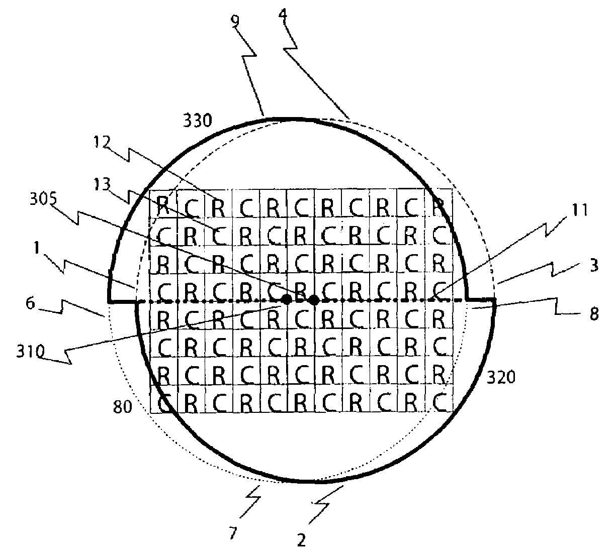
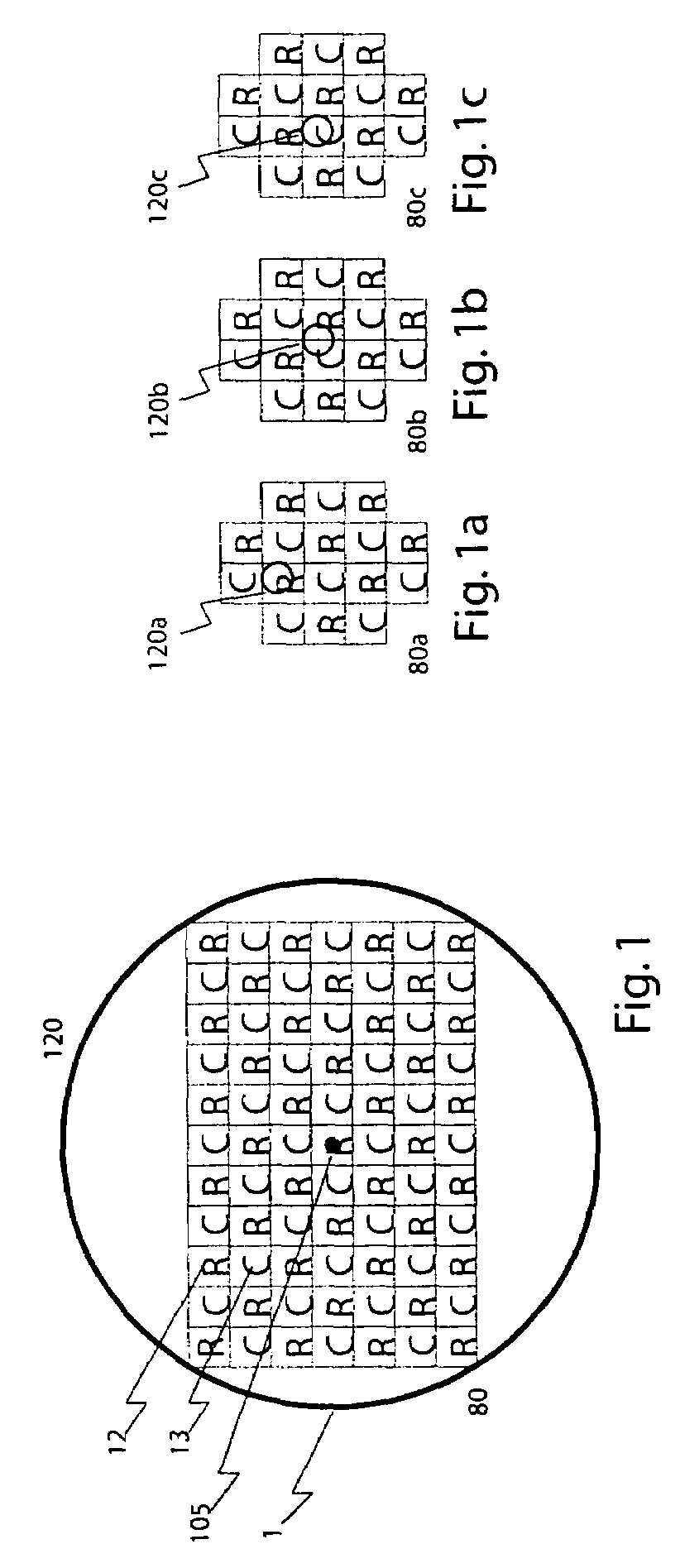
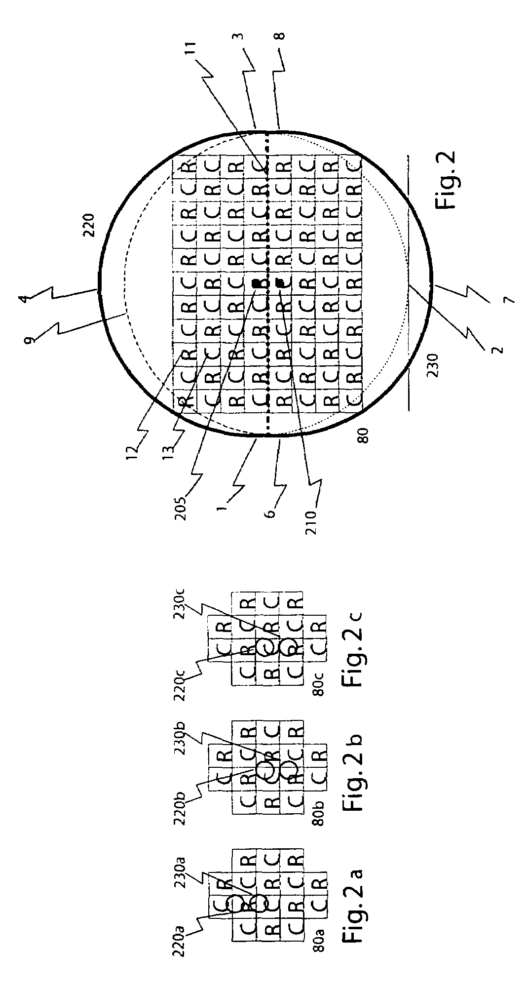
This approach enhances color accuracy and reduces artifacts by ensuring consistent illumination and area coverage across pixels, particularly for small details, without the need for excessive pixel density, thus maintaining high resolution and reducing the physical and cost-related issues associated with increased pixel counts.

Problems solved by technology

However, when small detail such as created by a fine pattern in a projected image or by small spots such as created by distant headlamps or tail lamps in the projected image, the system often has serious errors in the determination of colors for small details within the image.
Larger scale interference patterns often create particularly annoying artifacts in the resulting images.
Such systems are proprietary and have limitations in performance.
This approach is used for high end video cameras but requires multiple imagers and a quite complicated optical system.
The problem with this approach is that unless the blur spot is very large, the percentage of the light which falls on pixels of each color will vary considerably as the image assumes various positions on the sensing pixel array.
High resolution is normally a highly valued feature of an imager and the physical design problems and the cost of the imager and its associated image processing and image storage components increase with the number of pixels.
However, the technique is very expensive and in many implementations requires a relatively thick filter assembly which often adds distortion for lenses which are not typically designed to focus the image through a thick piece of transparent material.

Method used


Image

  • Optical elements, related manufacturing methods and assemblies incorporating optical elements
  • Optical elements, related manufacturing methods and assemblies incorporating optical elements
  • Optical elements, related manufacturing methods and assemblies incorporating optical elements

Examples


Embodiment Construction

[0035]Imaging systems are becoming commonplace in consumer electronics devices, residential systems, commercial systems and industrial applications. Consumer electronic devices include digital cameras, electronic video recorders, direct video devices (DVDs), digital video-telephones and the like. Residential systems include security systems, monitoring devices, surveillance systems, home entertainment systems and the like. Vehicle vision systems often incorporate imaging systems for equipment control, monitoring apparatus, warning devices and security systems. Industrial applications may include machine vision systems, control systems, monitory systems and the like.

[0036]Automatic vehicle exterior light control systems are described in commonly assigned U.S. Pat. Nos. 5,990,469, 6,008,486, 6,130,421, 6,130,448, 6,255,639, 6,049,171, 5,837,994, 6,403,942, 6,281,632, 6,291,812, 6,469,739, 6,399,049, 6,465,963, 6,587,573, 6,429,594, 6,379,013, 6,774,988, and U.S. patent application Ser...


PUM


Abstract

The present invention relates to various optical elements, related manufacturing methods and systems incorporating the optical elements. In at least one embodiment an optical element is provided that improves a vision systems capability to accurately measure a spectral characteristic of a distant light source.

Description

CROSS-REFERENCE TO RELATED APPLICATION[0001]This application claims priority under 35 U.S.C. §119(e) to U.S. Provisional Patent Application No. 60 / 495,906, confirmation number 2880, filed on Aug. 18, 2003, the entire disclosure of which is incorporated herein in its entirety by reference.BACKGROUND OF THE INVENTION[0002]The present invention relates to optics for imaging applications. It has become commonplace to employ digital imaging technology in a host of consumer electronic devices, residential systems, commercial systems and industrial applications. Often times, it is desirable to impart accurate color rendering in related devices and systems.[0003]For color imaging arrays, it is common to cover each pixel of the array with a color spectral filter so that each pixel will respond to the color determined by its associated spectral filter. In this way, each pixel responds only to a particular color or range of colors. A system of interpolation, extrapolation and / or averaging must...

Claims


Application Information

Patent Timeline
Patent Type & Authority Patents(United States)
IPC IPC(8): H01J3/14G01B11/14A61B8/02G02BH04N23/12H04N25/00
CPCG02B27/1013G02B27/1066G02B27/123G02B27/126H01L27/14625H04N3/1593H04N9/045G02B3/0006H01L27/14621H04N25/41H04N25/134
Inventor STAM, JOSEPH S.BECHTEL, JON H.
Owner GENTEX CORP
Learn More