Organic semiconductor element, production method therefor and organic semiconductor device
a production method and organic semiconductor technology, applied in the direction of semiconductor/solid-state device details, thermoelectric devices, transistors, etc., can solve the problems of difficult to make the area of a substrate larger, difficult to achieve expected characteristics, and difficult to make conduction between
- Summary
- Abstract
- Description
- Claims
- Application Information
AI Technical Summary
Problems solved by technology
Method used
Image
Examples
example 1
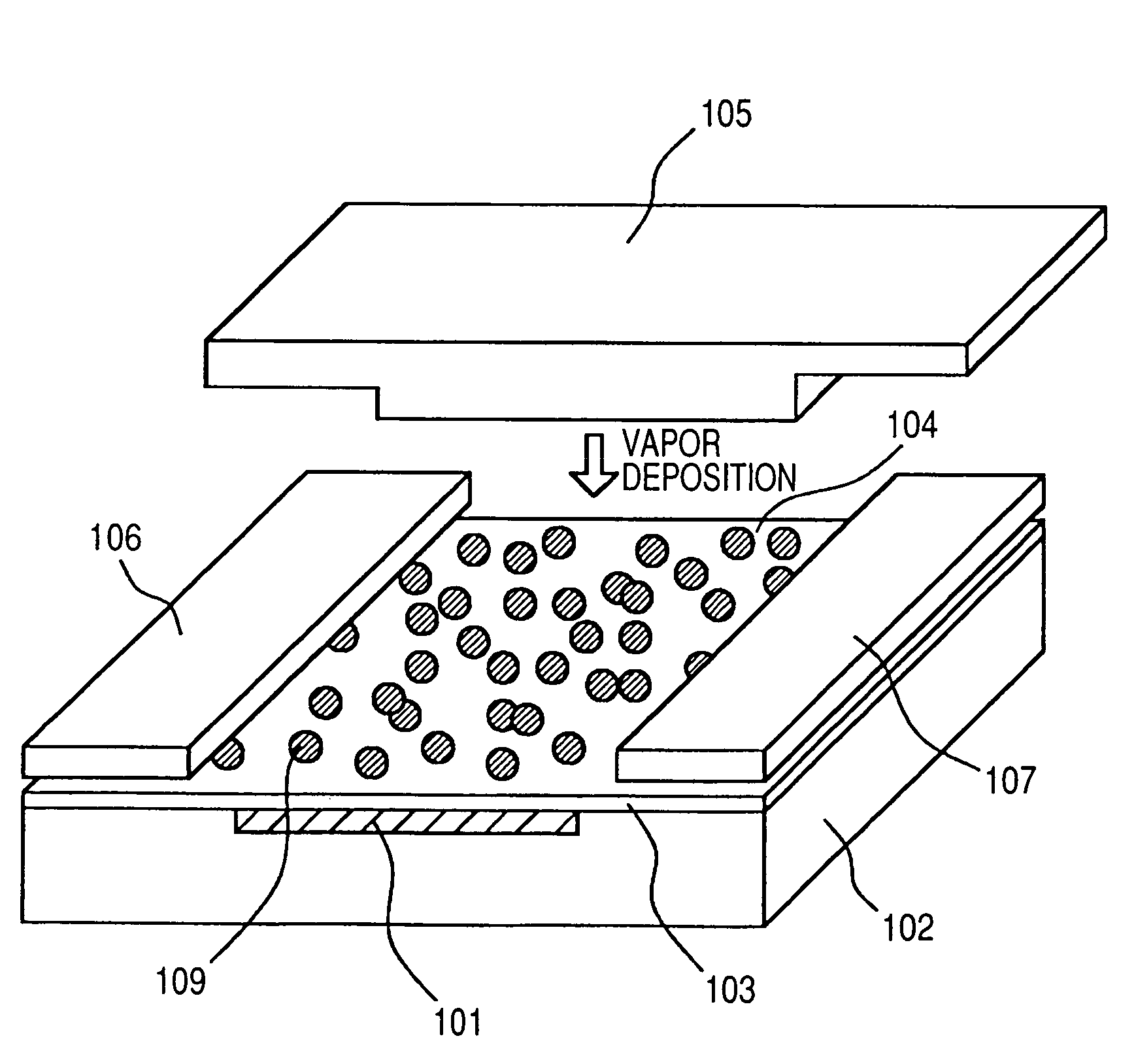
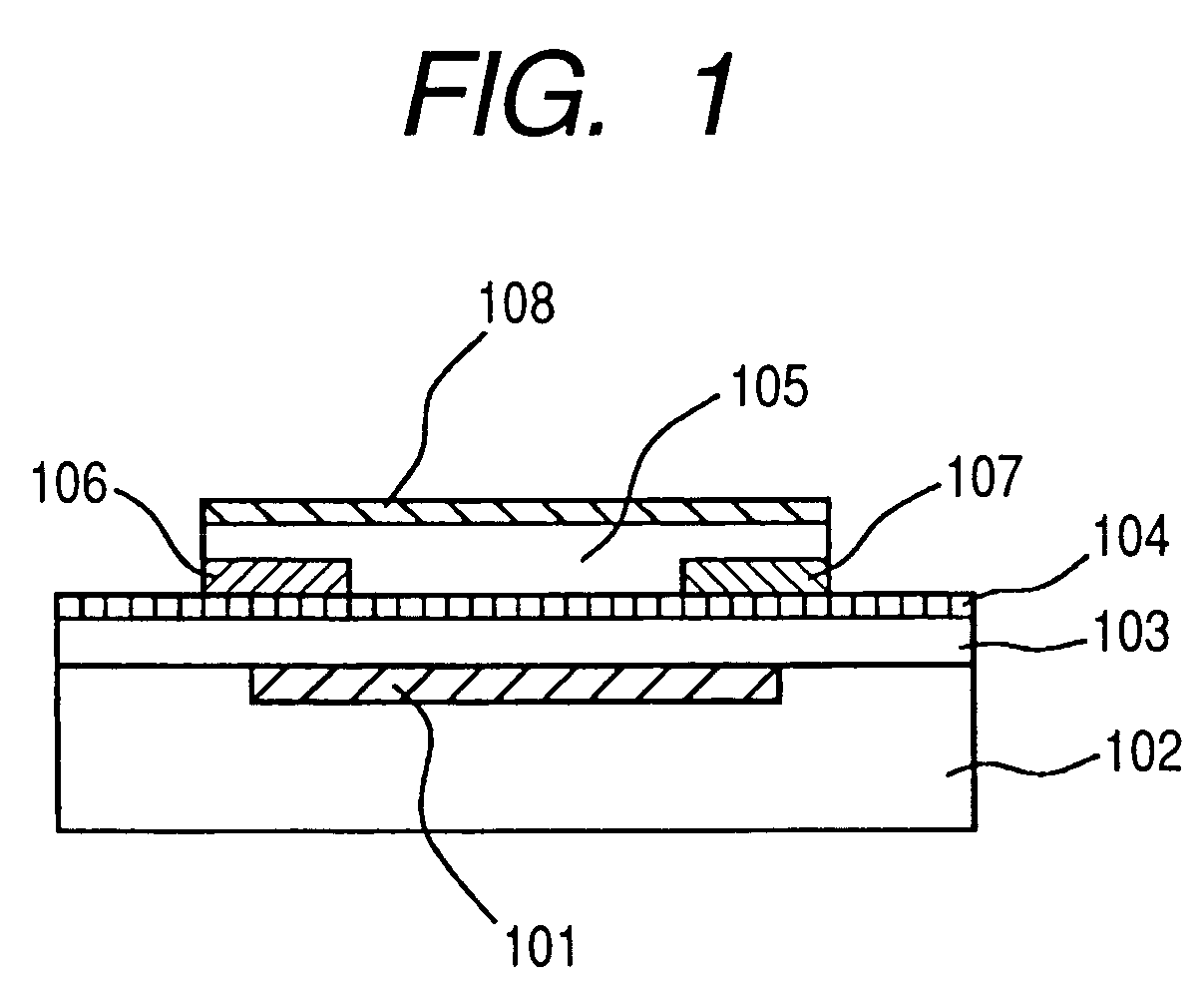
[0102]In the first place, description is made on the substrate used in the organic semiconductor device according to the present Example and the cleaning method.
[0103]The silicon substrate used in the present Example was a p-type substrate doped with boron. The resistivity of the substrate was 0.1 to 0.2 Ωcm. The crystal axis was .
[0104]A SiO2 film was formed on the silicon substrate. The SiO2 film was 200 nm in film thickness, which was formed on the surface of the silicon substrate by the wet thermal oxidation method. The oxidation conditions were the furnace temperature set at 95° C. and the inflow ratio of H2 and O2 set at 0.5.
[0105]The cleaning method of the silicon substrate was as follows. Twice repeated was the process in which silicon substrate was soaked in acetone with a purity of 99% or higher and subjected to ultrasonic cleaning for 5 min and then the substrate was soaked in purified water and subjected to ultrasonic cleaning for 5 min. After the cleaning, purified wate...
example 2
[0147]Description is made below on the embodiment in which the organic semiconductor element according to the present invention was utilized in an active matrix liquid crystal display device, with reference to FIGS. 10 through 12C.
[0148]FIG. 10 shows the active matrix liquid crystal display device according to the present invention.
[0149]FIG. 11 shows a sectional view of the active matrix liquid crystal display device taken along the line 11—11 of FIG. 10. Reference numeral 401 denotes a glass substrate, 402 a gate electrode, 403 a gate insulating film, 405 a source electrode, 406 a drain electrode, 407 a pentacene vapor-deposited film, 408 and 408′ signal wires, 409 and 409′ scanning wires, 410 a pixel electrode, 411 a SiNx protective film, 413 and 413′ oriented films, 414 a glass substrate, 415 an opposed electrode, 416 a liquid crystal composition, 417 a spacer bead, 418 and 418′ polarization plates, 419 a TFT substrate, and 420 an opposed substrate. Reference numeral 404 denotes...
example 3
[0155]Description is made on a production method of the IC information tag.
[0156]As for the explanation of FIG. 13, FIG. 13 shows a portion of an IC substrate. For simplicity of FIG. 13, only one inverted TFT is shown, but this one device is a large integrated array device. In FIG. 13. reference character 508 denotes a silicon substrate, 509 an organic semiconductor layer, 510 a resin insulating film. 512 a lower electrode, 514 a ferroelectric layer, 516 an upper electrode, 518 a resin insulating film, 528 an insulating film, 529 a metal wiring, 526 a conductive layer formed by embedding a metal in a through-hole, S a source electrode, and D a drain electrode. Additionally, the elements and the like shown in the figure are not accurately scaled. The IC information tag in the present Example has a structure in which an organic semiconductor is arranged on the downside, and a dielectric memory is stacked thereover. In the present invention, an organic dielectric memory is used, and tw...
PUM
 Abstract
Description
Claims
Application Information
 - R&D
- Intellectual Property
- Life Sciences
- Materials
- Tech Scout
- Unparalleled Data Quality
- Higher Quality Content
- 60% Fewer Hallucinations
Browse by: Latest US Patents, China's latest patents, Technical Efficacy Thesaurus, Application Domain, Technology Topic, Popular Technical Reports.
© 2025 PatSnap. All rights reserved.Legal|Privacy policy|Modern Slavery Act Transparency Statement|Sitemap|About US| Contact US: help@patsnap.com


