Amplifier circuit

Active Publication Date: 2007-03-27
QUALCOMM INC
View PDF18 Cites 34 Cited by
  • Summary
  • Abstract
  • Description
  • Claims
  • Application Information

AI Technical Summary

Benefits of technology

[0009]The control means may be operable to adjust the supply current I and the supply voltage V to maximise the amplifier efficiency in accordance with the variable desired output power level P, and to substantially maintain constant the amplifier efficiency over a range of amplifier output power levels P.
[0012]Thereby, the amplifier efficiency can be the same (i.e. near-ideal) for a wide range of output power levels. This is particularly advantageous for equipment that is required to operate at more than one output power level. This is achieved without requiring re-adjustment of the load impedance. In other words, a constant value of load impedance may be used for different output power levels without impairing the amplifier efficiency.
[0014]Also, if a battery is used for supplying power to the amplifier, by adjusting the voltage V input to the amplifier, rather than supplying the amplifier direct from the battery, the amplifier's efficiency is independent of a change of charge in the battery, e.g. as a result of battery discharge. A DC-to-DC converter could be used to provide the variable supply voltage. DC-to-DC converters have relatively high efficiency.
[0015]Furthermore, by adjusting both the input supply voltage and the supply current, the levels of generated harmonics in the case of non-class-A operation can be controlled more easily. That is, a symmetrical waveform can be produced for a wide range of output power levels, with voltage limiting and current limiting occurring at both peaks and troughs of the signal waveform. This reduces the level of second harmonic generated.

Problems solved by technology

However, a problem of this approach is that it is only possible, for a given load, to maintain near-optimum efficiency for the specified output power level for that load.
If an amplifier optimised for a specified output power level is used for a different power level, then a significant reduction in efficiency results if the amplifier is not re-adjusted (e.g. by adjusting the load).

Method used


Image

  • Amplifier circuit
  • Amplifier circuit
  • Amplifier circuit

Examples


Embodiment Construction

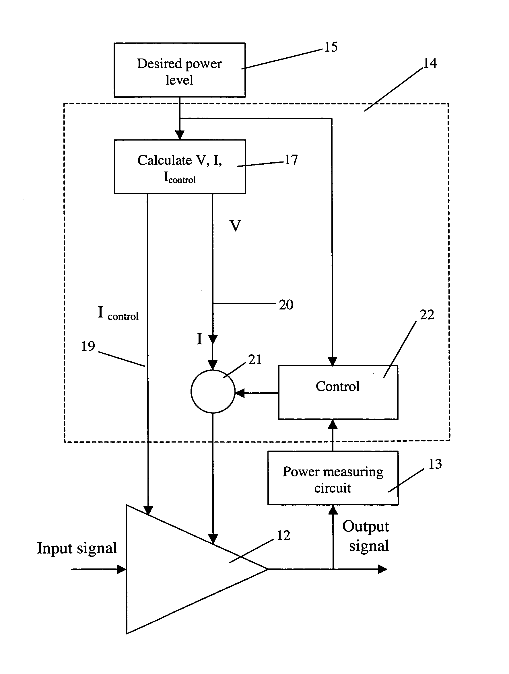
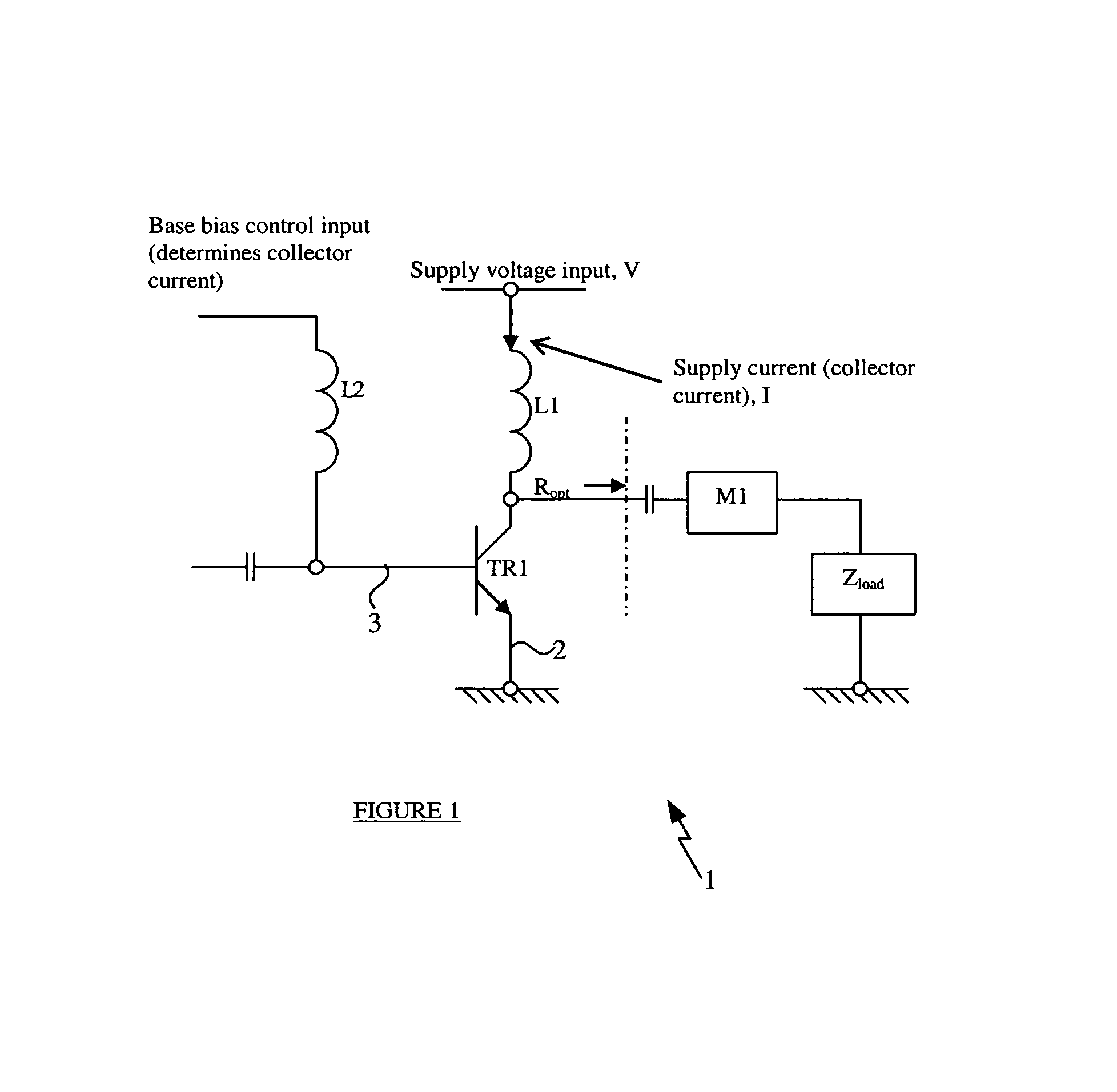
[0032]Referring to FIG. 1 of the accompanying drawings, there is shown an amplifier 1 comprising a NPN bipolar transistor TR1. An inductor L1 is connected to a collector terminal 2 of the transistor TR1. Likewise, an inductor L2 is connected to a base terminal 3 of the transistor TR1. A load Zload is connected to the collector terminal 2 via a lossless matching circuit M1. The lossless matching circuit transforms the load Zload into a completely real impedance Ropt. Accordingly, the effective load presented to the transistor collector is Ropt. Preferably, the matching circuit M1 includes any transistor parasitics (collector-emitter capacitance and load inductance) so that Ropt is the impedance presented to the transistor die. Ropt is called the dynamic load impedance and has the value of a pure resistance, measured in units of Ohms.

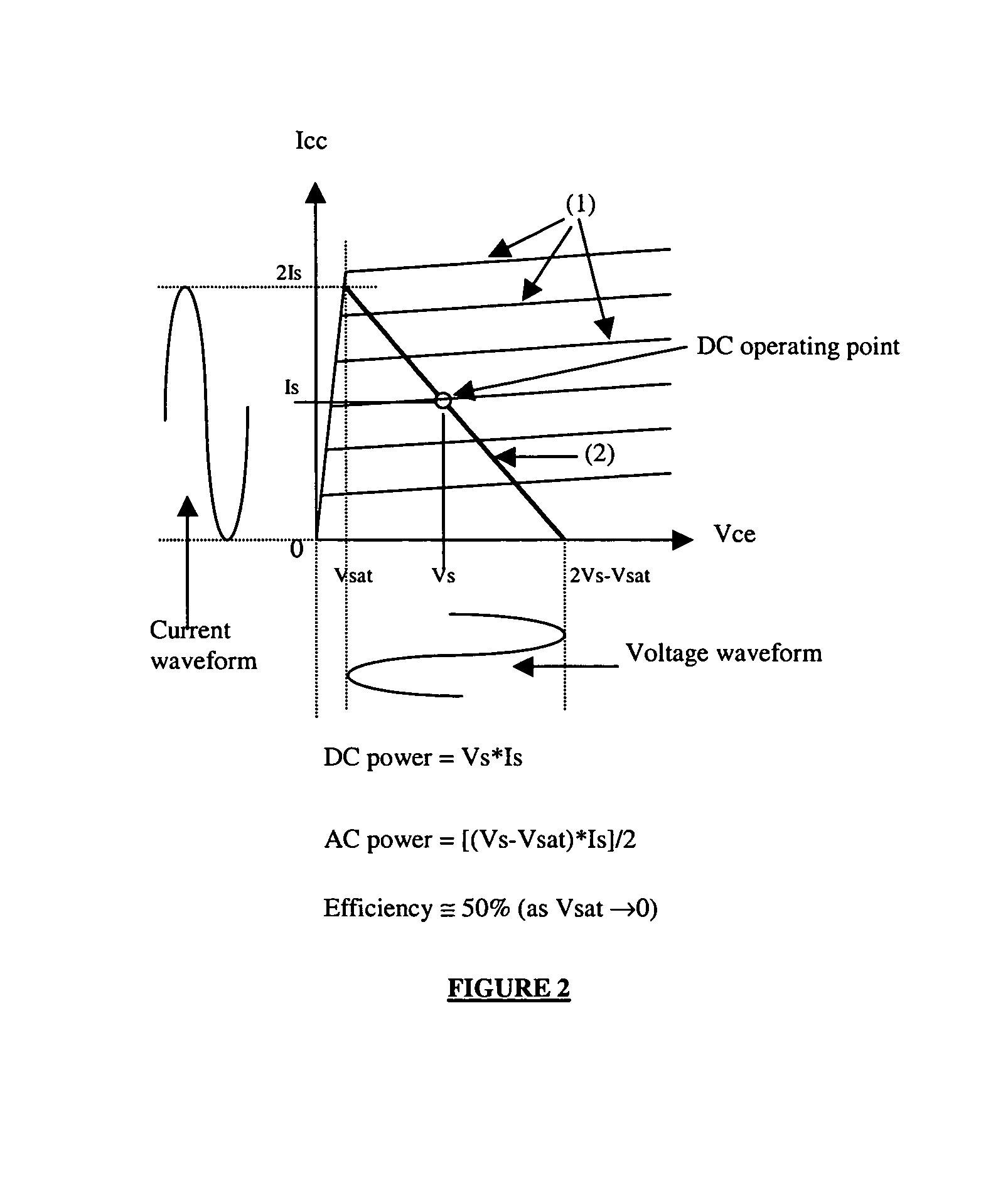
[0033]Referring now to FIG. 2, there are shown the collector characteristic curves 1 of the transistor TR1 together with dynamic load line 2. The horizon...


PUM


Abstract

An amplifier circuit 11 comprises an amplifier 12, an indicator of desired power 15, a power control circuit 14 and a power measuring circuit 13. The amplifier 12 amplifies an input signal to produce an output signal, and has an input for controlling a supply current I and an input for receiving a supply voltage V and supply current I, for driving the amplifier. The power control circuit calculates and applies values of both a supply voltage V and a supply current I, according to any one of a plurality of desired power levels, in order to operate the amplifier with maximum efficiency over a wide range of power levels. The power control circuit may further comprise a power control loop whereby adjustment of the output power can also be effected according to a measurement of output power and a desired level of output power.

Description

RELATED APPLICATIONS[0001]This application is a 371 of PCT / GB01 / 05182 filed on Nov. 23, 2001.[0002]The invention relates to an amplifier circuit and a method of operating an amplifier.BACKGROUND OF THE INVENTION[0003]Electronic amplifiers, and in particular power amplifiers, are widely used in audio equipment and in the transmitters of telecommunication transceivers. One of the requirements for such amplifiers is to obtain the best possible efficiency. For the purpose of this description, amplifier efficiency can be regarded as the ratio between alternating-current (AC) output power and direct-current (DC) input power supplied to the amplifier.[0004]In known amplifiers, this requirement is addressed by first specifying the required output power level, and then optimising the amplifier for that specific output power level. One known way of optimising the amplifier is to select an optimum load for the required output power level. Another is to employ a switchable load that can be adju...

Claims


Application Information

Patent Timeline
IPC IPC(8): H03F3/04H03F1/02
CPCH03F1/0233
Inventor HARRIS, MARK V.
Owner QUALCOMM INC
Why Eureka
Try Eureka