Integrated process condition sensing wafer and data analysis system

a technology of process condition and data analysis, applied in the field of integrated process condition sensing wafer and data analysis system, can solve the problems of failure completely, failure of subsequent integrated circuit or device, and substandard performance of subsequent integrated circuit or device, and achieve the effect of high integration, reducing the amount of data needed, and reducing the size required

Inactive Publication Date: 2006-11-14
SENSARRAY CORP
View PDF55 Cites 79 Cited by
  • Summary
  • Abstract
  • Description
  • Claims
  • Application Information

AI Technical Summary

Benefits of technology

[0010]PCMDs may be made compatible with harsh environments by protecting components from chemical or electrical damage. Critical components may have covers similar to parts used in packaging ICs. Covers may also be made of specialized materials such as sapphire or, for electrical protection, silicon or metal. PCMDs may also be adapted to high temperatures by incorporating a temperature compensating circuit to allow an oscillator to perform outside its specified temperature range.
[0011]A handling system provides a docking station or base for a PCMD. The PCMD exchanges data with an electronics module when it is docked in the handling system and also receives power from the electronics module. The handling system may comprise an electronics module within a standard substrate carrier such as a front opening unified pod (FOUP). This allows the handling system to be highly integrated with a tool or with facility automation. The PCMD may be moved to and from the FOUP by the tool and the FOUP may be moved from one tool to another by the facility automation. The FOUP provides a clean environment for the PCMD where it may be stored or transported. In addition, loading stations for FOUPs are normally provided with RFID readers to determine the identity of the FOUP and relay the information to a tracking system via a network. By connecting the electronics module in the FOUP to an RFID transceiver, data from the electronics module may be sent to the network where it may be accessed.
[0012]Data acquired from the sensors may be compressed by the electronic system on the PCMD prior to non-volatile storage and / or transmission of the data. The data are represented by temporal and / or spatial differences, thereby significantly reducing the amount of data necessary to represent the sensor measurements. Storage of certain of the acquired data may also be omitted if the condition being monitored by the sensors meets certain criteria. A reduction in the amount of data reduces the size required for a non-volatile memory on the PCMD, conserves its battery power and extends the period of time (runtime) that the PCMD may operate to acquire data between battery charges.
[0013]A handling system may have an alignment module that may move a PCMD within a handling system in order to facilitate communication between the PCMD and the electronics module of the handling system, as well as charging the PCMD battery. Vertical and rotational motion of a PCMD may be achieved by a rotation stage or wheels supporting its perimeter. Raising a PCMD may allow better coupling to the electronics module. Lateral movement of the PCMD may be achieved by a moving belt or wheel that is brought into contact with the lower surface of the PCMD to move the PCMD into position. As an alternative to raising the wafer, a flexible sheet containing a battery charging and / or communication coil may be attached to the underside of the electronics module in a manner so that it may be lowered onto the exposed surface of the PCMD.

Problems solved by technology

Any deviation from optimal processing conditions may cause the ensuing integrated circuit or device to perform at a substandard level or, worse yet, fail completely.

Method used


Image

  • Integrated process condition sensing wafer and data analysis system
  • Integrated process condition sensing wafer and data analysis system
  • Integrated process condition sensing wafer and data analysis system

Examples


Embodiment Construction

[0057]The measurement system in one embodiment measures processing conditions in various locations of a wafer or substrate and records them in memory for later transmission or downloading of the process conditions. In another embodiment of the measurement system where a processing chamber has windows capable of data transmission, the system is additionally capable of transmitting the processing conditions in real time to a data processing device.

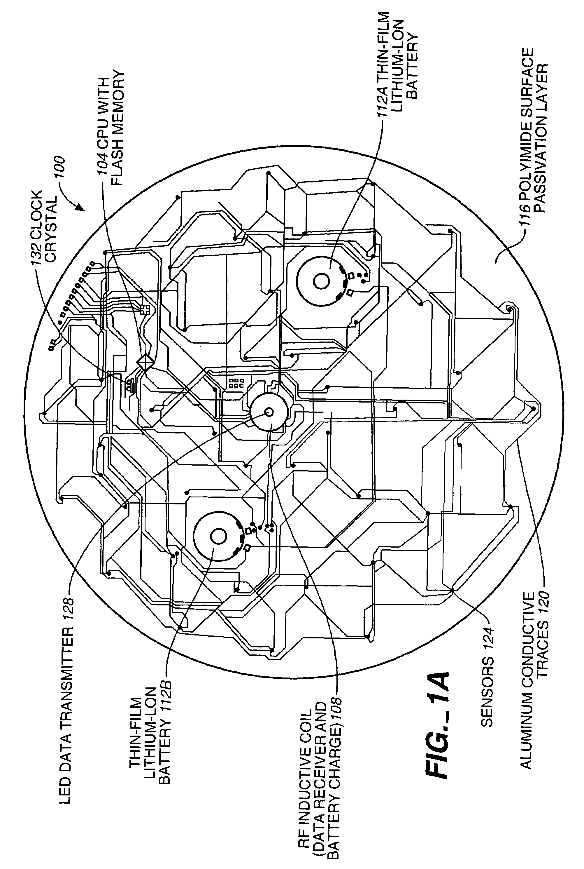
[0058]FIG. 1A illustrates process condition measuring device (“PCMD”) 100, an embodiment of the present invention. PCMD 100 is part of a process measurement system, the other components of which will be described later with reference to FIG. 2. PCMD 100 comprises a substrate such as a silicon wafer, glass substrate, or other substrates well known in the art. Substrate 102 (not visible in plan view) is preferably a silicon wafer and may be of any diameter but is preferably an 8 or 12 inch diameter wafer. The diameter is preferably that of waf...


PUM


Abstract

A process condition measuring device and a handling system may be highly integrated with a production environment where the dimensions of the process condition measuring device are close to those of a production substrate and the handling system is similar to a substrate carrier used for production substrates. Process conditions may be measured with little disturbance to the production environment. Data may be transferred from a process condition-measuring device to a user with little or no human intervention.

Description

CROSS-REFERENCE TO RELATED APPLICATIONS[0001]This is a continuation-in-part of patent application Ser. No. 10 / 718,269, filed Nov. 19, 2003, which claims the benefit of U.S. Provisional Patent Application No. 60 / 430,858 filed on Dec. 3, 2002, U.S. Provisional Patent Application No. 60 / 496,294 filed on Aug. 19, 2003, and U.S. Provisional Patent Application No. 60 / 512,243 filed on Oct. 17, 2003. The benefits of the filing dates of provisional applications Nos. 60 / 496,294 and 60 / 512,243 are also being directly claimed herein. Each of these applications is also incorporated herein in its entirety for all purposes by this reference.BACKGROUND OF THE INVENTION[0002]1. Field of the Invention[0003]The present invention relates to semiconductor wafer processing, LCD display glass substrate processing, magnetic memory disc processing, and other devices fabricated from thin film processes, and, more specifically, to a system that can sense and record processing conditions and transmit data to a...

Claims


Application Information

Patent Timeline
Patent Type & Authority Patents(United States)
IPC IPC(8): G01R31/28G01R31/02H01L21/00
CPCH01L21/67253H01L21/6732H01L21/681H01L2224/48091H01L2224/48227H01L2924/01078H01L2924/15153H01L2924/15157H01L2924/15165H01L2924/16152H01L2924/16153H01L2924/16195H01L2924/19041H01L2924/3011H01L2924/3025H01L2924/00014H01L2924/01087H01L2924/12041H01L2924/10253H01L2924/00H01L22/00
Inventor RENKEN, WAYNE GLENNJENSEN, EARL M.GORDON, ROYPAQUETTE, BRIANSUN, MEI H.
Owner SENSARRAY CORP
Why Eureka
Try Eureka