Clock generator for pseudo dual port memory

a dual-port memory and clock signal technology, applied in the field of memory timing, can solve the problem of insufficient clock signal to be generated soon, and achieve the effect of preventing signal degradation

Inactive Publication Date: 2006-06-13
AVAGO TECH INT SALES PTE LTD
View PDF6 Cites 6 Cited by
  • Summary
  • Abstract
  • Description
  • Claims
  • Application Information

AI Technical Summary

Benefits of technology

[0007]Accordingly, the present invention is directed to a circuit and method for preventing signal degradation for a clock signal supplied to a pseudo dual port memory.
[0010]Several advantages are provided by the present invention. An advantage is that the port B (write) clock ICLKB is not related to CLK falling edge. The port B clock ICLKB is generated after A (read) port operation by the RESET signal that is generated by a timing block (e.g. a self time block) or some other control block. The port B clock ICLKB will make B port (write) operation start just after A (read) port operation regardless of CLK falling edge. Other advantages include minimization of the clock cycle time and operation unaffected by the duty ratio of an external clock. The port B address and input data can be latched with sufficient set up and hold times by using ICLKB as a feedback control and the delaying effect of other circuit elements.

Problems solved by technology

The dual port memory timing circuit of FIG. 4 works well at slower clock speeds, but is insufficient for higher clock soon to be achieved for input / output data transfers to a pseudo dual port memory.

Method used


Image

  • Clock generator for pseudo dual port memory
  • Clock generator for pseudo dual port memory
  • Clock generator for pseudo dual port memory

Examples


Embodiment Construction

[0017]Reference will now be made in detail to the presently preferred embodiments of the invention, examples of which are illustrated in the accompanying drawings.

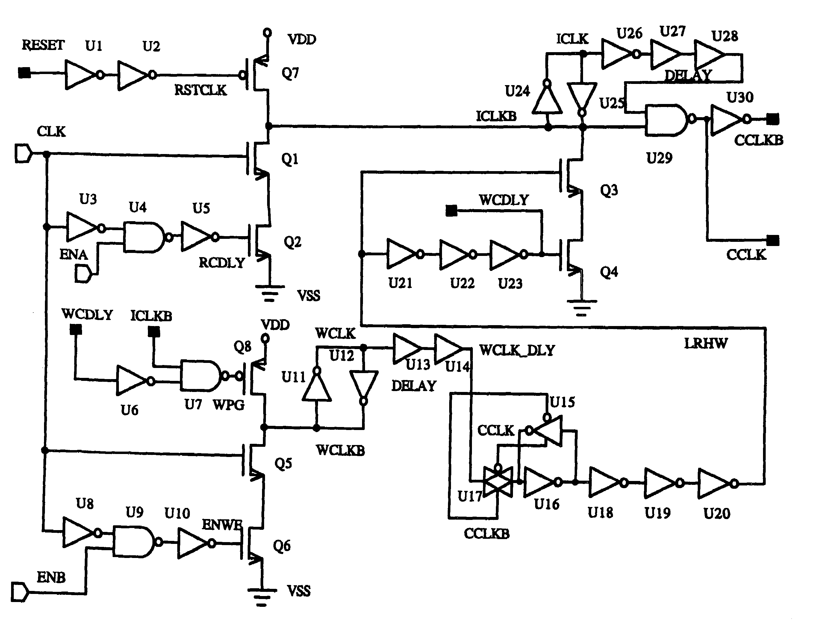
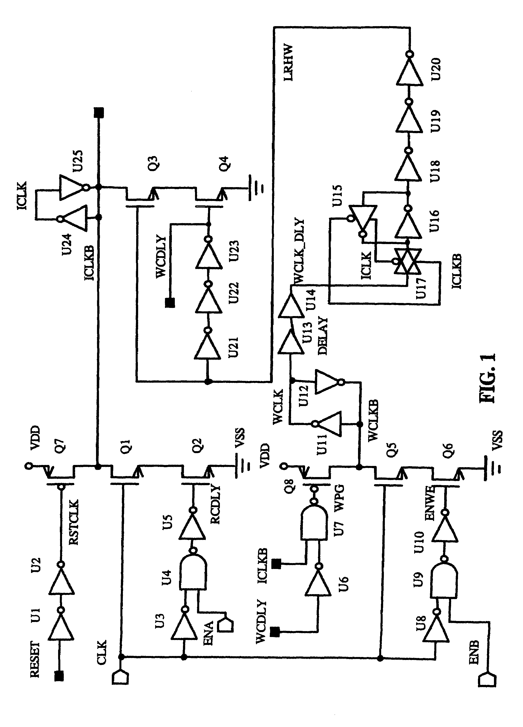
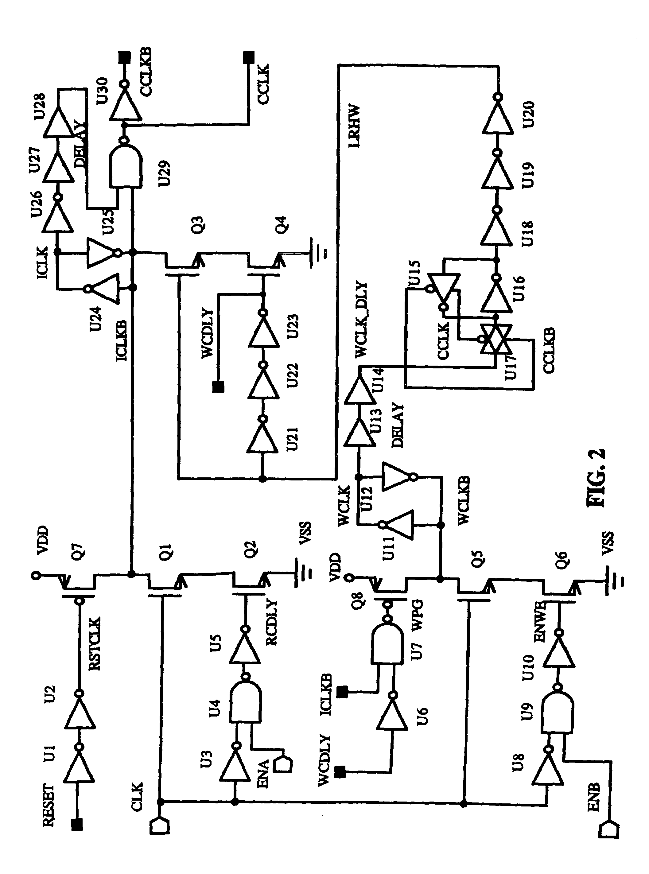
[0018]The present invention is directed to a circuit and method for preventing timing signal degradation for a pseudo dual port memory port. Through a system of delay and latch circuitry, the present invention permits a read operation to be performed and terminated before a write operation is performed. Adjustability may be achieved through such techniques as adjusting the number of delay elements. Timing feedback is provided to ensure that the write signal is temporally separated from the read signal.

[0019]FIG. 1 shows an embodiment of a clock generator circuit for a dual port memory of the present invention. The basic inputs to the circuit include a reset signal, a clock signal CLK, a read enable signal ENA, and a write enable signal ENB. The basic outputs of the circuit are one or two clock signals ICLKB / ICLK or CCLKB / C...


PUM


Abstract

A clock generating circuit for a pseudo dual port memory incorporates feedback, delays, and latches to ensure that the write (read) operation clock pulse is sufficiently spaced in time from the read (write) operation clock. The clock generating circuit receives an external clock, a read enable signal, a write enable signal, and a reset signal as inputs. Advantages include minimization of the clock cycle time and operation unaffected by the duty ratio of an external clock. Delay circuitry may be added such that the generated clock signal has sufficient fan out and is sufficiently stable.

Description

CROSS REFERENCE TO RELATED APPLICATIONS[0001]The present application is a Divisional Application of U.S. patent application Ser. No. 10 / 397,483 filed Mar. 25, 2003 now U.S. Pat. No. 6,809,983 issued on Oct. 26, 2004. Said U.S. patent application Ser. No. 10 / 397,483 is hereby incorporated by reference.FIELD OF THE INVENTION[0002]The present invention generally relates to the field of memory timing, and particularly to a circuit and method for generating clock signals for a pseudo dual port memory.BACKGROUND OF THE INVENTION[0003]Dual or multi port memory is usually much lower density than single port memory because of the core cell structure. To increase the dual (multi) port memory density, pseudo dual port memory can be used. Although the external operation of pseudo dual port memory resembles the operation of true dual port memory, pseudo dual port memory incorporates a single port core cell. Pseudo dual port memory should perform multiple read and / or write operations within a sin...

Claims


Application Information

Patent Timeline
Patent Type & Authority Patents(United States)
IPC IPC(8): G11C8/00G11C7/22
CPCG11C7/222G11C7/22
Inventor JUNG, CHANG HO
Owner AVAGO TECH INT SALES PTE LTD
Why Eureka
Try Eureka