Corner cube array and method of making the corner cube array

a technology of corner cubes and arrays, which is applied in the field of corner cube arrays and a method of making corner cube arrays, can solve the problems of difficult to make an array of corner cubes, difficult to make a corner cube of a small size, and the prism to be formed by this method cannot have any other shape, etc., and achieves the effect of high shape precision and small siz

Active Publication Date: 2006-05-16
SHARP KK
View PDF19 Cites 18 Cited by
  • Summary
  • Abstract
  • Description
  • Claims
  • Application Information

AI Technical Summary

Benefits of technology

[0015]In order to overcome the problems described above, an object of the present invention is to provide a corner cube array having a very small size and a high shape precision and a method of making such a corner cube array.
[0033]In one preferred embodiment of the present invention, the step of adjusting the shape of the exposed surface area of the substrate preferably includes the step of reducing unnecessary crystallographic planes, other than {100} planes of the crystalline material, in the exposed surface area of the substrate.
[0037]In yet another preferred embodiment, the step of adjusting the shape of the exposed surface area of the substrate preferably includes the step of supplying a second active species, which includes an element that is contained in the crystalline material and which is either the same as, or different from, the first active species, onto the substrate, thereby further growing the crystals anisotropically.
[0038]In yet another preferred embodiment, the step of performing the first patterning process preferably includes the step of removing portions of the exposed surface area of the substrate, and the step of performing the second patterning process preferably includes the step of supplying a second active species, which includes an element that is contained in the crystalline material and which is either the same as, or different from, the first active species, onto the substrate, thereby further growing the crystals anisotropically.

Problems solved by technology

Thus, it is difficult to make an array of corner cubes of as small a size as about 100 μm or less by this method.
Thus, it is actually difficult to make a corner cube of a small size.
However, the prisms to be formed by this method can have no other shape but the triangular pyramidal shape.
In that case, color mixture and other problems may occur.
However, according to any of the above-described mechanical methods of making corner cubes such as the plate method and the pin bundling method, it is often difficult to make corner cubes of such a small size as intended due to some variations that should occur in an actual manufacturing process.
As a result, the efficiency of retro-reflection may decrease disadvantageously.
Furthermore, it is impossible to make a cubic corner cube, having a three-dimensional shape as a combination of convex and concave portions and consisting of three square planes that are opposed substantially perpendicularly to each other, by the triangular prism method.
Also, as for a micro corner cube obtained by a photochemical method as disclosed in Japanese Laid-Open Publication No. 7-205322, it is difficult to ensure high plane precision (i.e., planarity).
Actually, though, such strict process control is hard to realize.
Thus, it is not easy to make a micro corner cube array in its intended shape by such a method, either.

Method used


Image

  • Corner cube array and method of making the corner cube array
  • Corner cube array and method of making the corner cube array
  • Corner cube array and method of making the corner cube array

Examples


embodiment 1

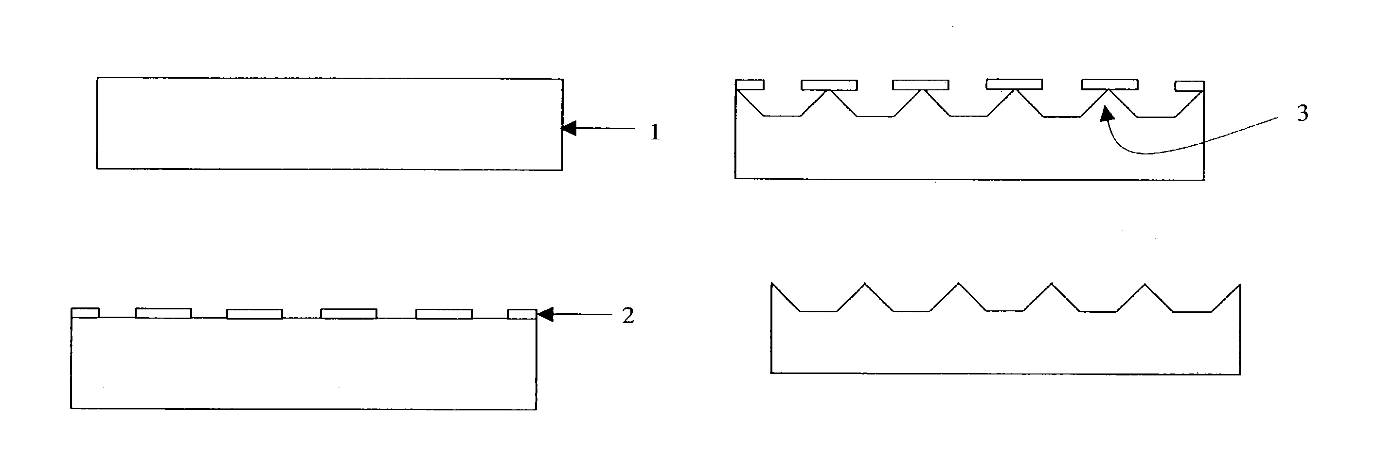
[0063]In a first specific preferred embodiment of the present invention, a substrate, made up of GaAs crystals having a sphalerite structure, is used as a cubic single crystalline substrate. The solid shape elements are formed on this substrate by a wet etching process so as to define a predetermined pattern thereon, and then an anisotropic crystal growth process is carried out on the solid shape elements on the substrate, thereby forming a micro corner cube array thereon.

[0064]FIGS. 1A through 1E and FIGS. 2A through 2E show respective process steps for making a micro corner cube array according to the first preferred embodiment of the present invention. First, as shown in FIGS. 1A and 2A, a GaAs substrate 1, of which the surface is substantially parallel to {111}B planes, is prepared, and has that surface mirror-polished. It should be noted that {111}A planes are formed by gallium atoms, while {111}B planes are formed by arsenic atoms.

[0065]Next, as shown in FIGS. 1B and 2B, the s...

embodiment 2

[0087]Hereinafter, a second specific preferred embodiment of the present invention will be described.

[0088]In this second preferred embodiment, solid shape elements (i.e., convex portions in this preferred embodiment also) are formed by a wet etching process so as to define a predetermined pattern on the surface of a GaAs substrate. Then, those solid shape elements are dry-etched while active species, including the elements contained in the crystalline material of the substrate, are supplied onto the substrate, thereby forming a micro corner cube array.

[0089]FIGS. 6A through 6E and FIGS. 7A through 7E show respective process steps for making a micro corner cube array according to the second preferred embodiment of the present invention. First, as shown in FIGS. 6A and 7A, a GaAs substrate 21, of which the surface is substantially parallel to {111}B planes, is prepared, and has that surface mirror-polished as in the first preferred embodiment described above.

[0090]Next, as shown in F...

embodiment 3

[0102]In the first and second preferred embodiments described above, in the process step of supplying the first active species, an anisotropic crystal growth process is carried out on the solid shape elements on the substrate, thereby forming a plurality of corner cube unit elements, each being made up of three crystal planes that are defined by {100} planes. However, just by performing such an anisotropic crystal growth process, other families of crystal planes may be left on the exposed surface of the substrate.

[0103]Specifically, in the process step of supplying the first active species according to the first or second preferred embodiment described above, unnecessary families of crystal planes, other than the {100} planes to be defined, likely remain around the vertices of the respective unit elements. Even if the surface of the substrate is further patterned (e.g., etched) to reduce the percentage of those unnecessary families of crystal planes, other unnecessary families of cr...


PUM

PropertyMeasurementUnit
Optical reflectivityaaaaaaaaaa
Sizeaaaaaaaaaa
Shapeaaaaaaaaaa

Abstract

A method of making an array of corner cubes includes the steps of: preparing a substrate, at least a surface portion of which is made of a cubic crystalline material and which has a surface that is substantially parallel to {111} planes of the crystalline material; and patterning the surface of the substrate such that a plurality of solid shape elements defines a predetermined pattern on the surface of the substrate. Each of the solid shape elements is defined by a number of concave portions, a number of convex portions or a combination of concave and convex portions. The method further includes the step of supplying a first active species, including an element that is contained in the crystalline material, onto the substrate on which the solid shape elements have been formed.

Description

BACKGROUND OF THE INVENTION[0001]1. Field of the Invention[0002]The present invention relates to a corner cube array and a method of making the corner cube array. More particularly, the present invention relates to a method of making a corner cube array of a very small size, which can be used effectively in a display device, for example.[0003]2. Description of the Related Art[0004]In recent years, various types of optical elements having extremely small sizes (i.e., so-called “micro optical elements”), including microlenses, micro mirrors and micro prisms, have been developed and applied more and more extensively to the fields of optical communications and display devices. It is expected that the optical technology and display technology will be further developed and advanced by realizing those micro optical elements.[0005]Examples of such optical elements include a corner cube reflector, which is formed by arranging a plurality of corner cubes as an array with a regular pattern. Ea...

Claims


Application Information

Patent Timeline
IPC IPC(8): G02F1/1335G02B5/122G02B1/02G02B5/124
CPCG02B5/124Y10T428/1095Y10T428/24479C09K2323/061G02F1/1335
Inventor IHARA, ICHIROMINOURA, KIYOSHI
Owner SHARP KK
Why Eureka
Try Eureka