
Biologic electrode array with integrated optical detector

a biological electrode array and optical detector technology, applied in the field of electrochemical systems, can solve the problems of arbitrarily slow update rate, and achieve the effect of enhancing the reaction progression and minimizing the utilization of off-chip control circuitry

Inactive Publication Date: 2006-05-16
GAMIDA FOR LIFE
View PDF33 Cites 176 Cited by
  • Summary
  • Abstract
  • Description
  • Claims
  • Application Information

AI Technical Summary

Benefits of technology

[0015]In view of the foregoing, it will be appreciated that a biologic array in accordance with the present invention provides for very precise control of the potentials / currents delivered to individual electrodes within the array, while minimizing the utilization of “off-chip” circuitry and overall system costs. Further, by using local sample-and-hold circuits (or other local memory circuits) to control the level of electrical stimulus applied to particular test sites, arrays in accordance with the present invention may achieve a level of stimulus specificity and electrode utilization far superior to that achieved using most prior art systems.
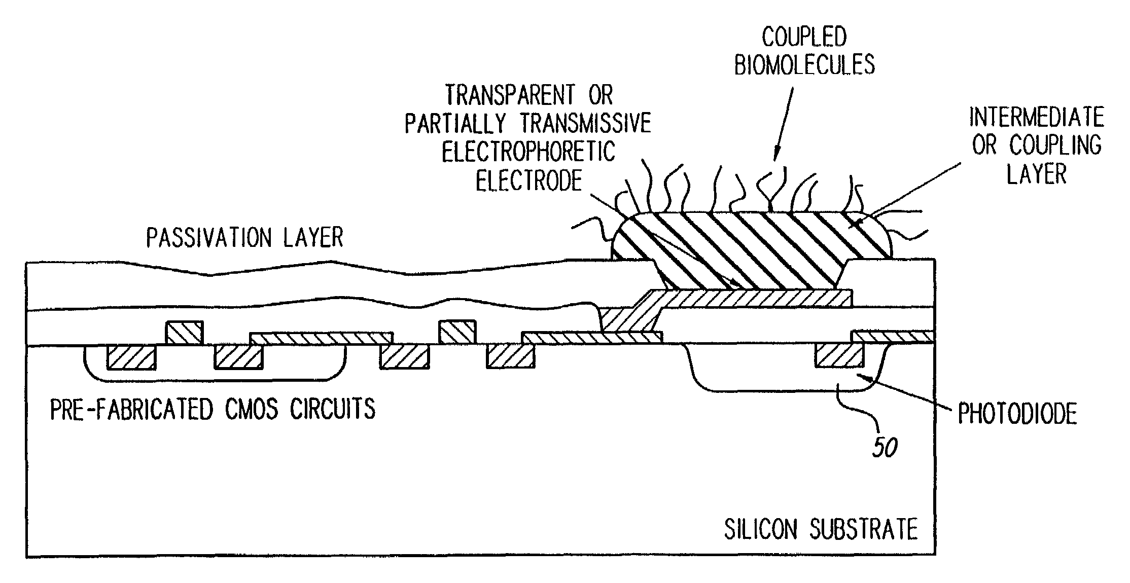
[0017]Finally, in still another innovative aspect, the present invention provides for the incorporation of optical fluorescence or absorption detection circuitry within a biologic electrode array matrix to improve coupling of emitted photons into the detection electronics. More specifically, in accordance with one embodiment of the present invention, a biologically active electrode is formed above a suitable optical detector such as a MOS-photodiode structure within, for example, a CMOS circuit. In such an embodiment, the electrode may be formed from a substance which is at least partially transparent, or the electrode may be formed in such a fashion that it permits the passage of light through its body to an underlying photodetector.
[0021]It is another object of the present invention to provide an improved biologic electrode array which is compact and minimizes the utilization of off-chip control circuitry, even for large numbers of electrodes.
[0022]It is another object of the present invention to provide an improved biologic electrode site which includes a sample-and-hold circuit, and which may be fabricated using conventional CMOS semiconductor fabrication techniques.
[0023]It is still another object of the present invention to provide an improved biologic electrode array which includes heating elements for enhancing the progression of reactions such as DNA amplification in situ.

Problems solved by technology

If non-volatile sample-and-hold circuits are used (i.e., if EEPROM or some equivalent technology is utilized), such decays may not be significant, allowing for arbitrarily slow update rates.

Method used


Image

  • Biologic electrode array with integrated optical detector
  • Biologic electrode array with integrated optical detector
  • Biologic electrode array with integrated optical detector

Examples


Embodiment Construction

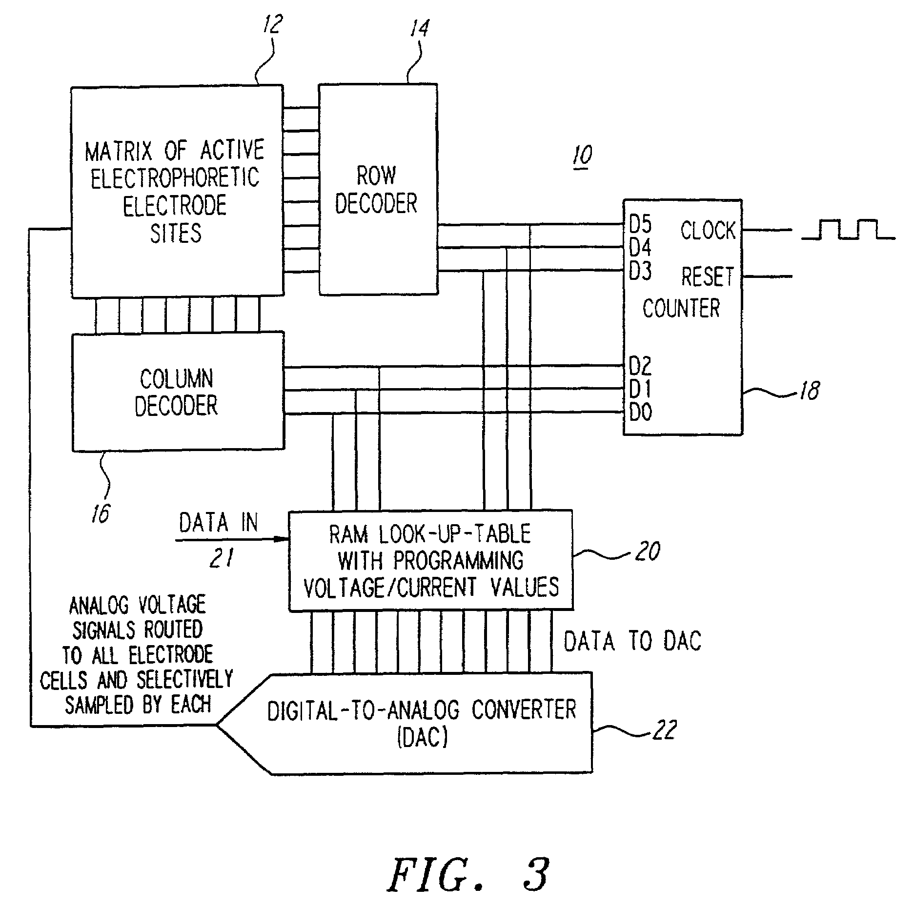
[0037]Turning now to the drawings, as shown in FIG. 3, a biologic array 10 in accordance with one preferred form of the present invention may comprise a matrix of active biologic electrode sites 12, a row decoder 14, a column decoder 16, a counter 18, a random access memory (RAM) 20 acting as a look-up table, and a digital-to-analog converter (DAC) 22. In a preferred form, each of the above listed elements may be disposed on a single semiconductor chip, and the entire array 10 may be fabricated using conventional CMOS semiconductor fabrication techniques. Further, in the presently preferred form a computer (not shown) may be used to load data, as needed, into the RAM 20 via, for example, a data input port 21.

[0038]Turning now also to FIG. 4(a), each biologic electrode site 24, which makes up the matrix of biologic electrodes 12, may comprise a sample-and-hold circuit 26, an amplifier 28 and an electrode 30. In one preferred form, the sample-and-hold circuit 26 may comprise a capacit...


PUM


Abstract

A biologic electrode array is formed on a semiconductor substrate. A matrix of electrode sites is disposed on the semiconductor substrate. A matrix of optical detectors is disposed beneath the electrode sites in the semiconductor substrate, wherein each electrode site is associated with a corresponding optical detector. The optical detectors are coupled to detection circuitry formed on the semiconductor substrate. The electrode sites may include slitted electrodes, punctuated electrodes, or optically transparent electrodes.

Description

[0001]This application is a continuation of U.S. application Ser. No. 09 / 903,110, filed on Jul. 10, 2001, now issued as U.S. Pat. No. 6,682,936, which is a continuation of U.S. application Ser. No. 09 / 364,676, filed Jul. 30, 1999, now issued as U.S. Pat. No. 6,258,606, which is a continuation of U.S. application Ser. No. 08 / 677,305, filed on Jul. 9, 1996, now issued as U.S. Pat. No. 5,965,452, all of which are incorporated by reference as if set forth fully herein.FIELD OF THE INVENTION[0002]The present invention relates generally to electronic systems for carrying out and / or monitoring biologic reactions and, more particularly, to the design, fabrication and uses of self-addressable, self-assembling microelectronic systems for carrying out and controlling multi-step and multiplex reactions in microscopic formats.BACKGROUND OF THE INVENTION[0003]For some time now, substantial attention has been directed to the design, implementation and use of array-based electronic systems for carr...

Claims


Application Information

Patent Timeline
Patent Type & Authority Patents(United States)
IPC IPC(8): G01N21/01G01N27/26G01N27/27G01N27/327G01N27/453B01J19/00G01N27/00G01N27/403G01N33/543
CPCB01J19/0046G01N33/5438G01N27/3276Y10T436/144444B01J2219/00585B01J2219/00596B01J2219/00605B01J2219/00612B01J2219/00617B01J2219/00621B01J2219/00637B01J2219/00653B01J2219/00659B01J2219/00722G01N27/27Y10T436/143333Y10T436/170769Y10T436/173845Y10T436/171538Y10T436/203332Y10T436/200833Y10T436/17Y10T436/20Y10T436/142222B01J2219/00527G01N33/543
Inventor KOVACS, GREGORY T. A.
Owner GAMIDA FOR LIFE
Learn More