Light emitting device of III-V group compound semiconductor and fabrication method therefor
a technology of compound semiconductor and light emitting device, which is applied in the direction of semiconductor devices, basic electric elements, electrical apparatus, etc., can solve the problems of restricted light extraction from the light emitting device, and achieve the effect of improving the efficiency of external light extraction
- Summary
- Abstract
- Description
- Claims
- Application Information
AI Technical Summary
Benefits of technology
Problems solved by technology
Method used
Image


Examples
first embodiment
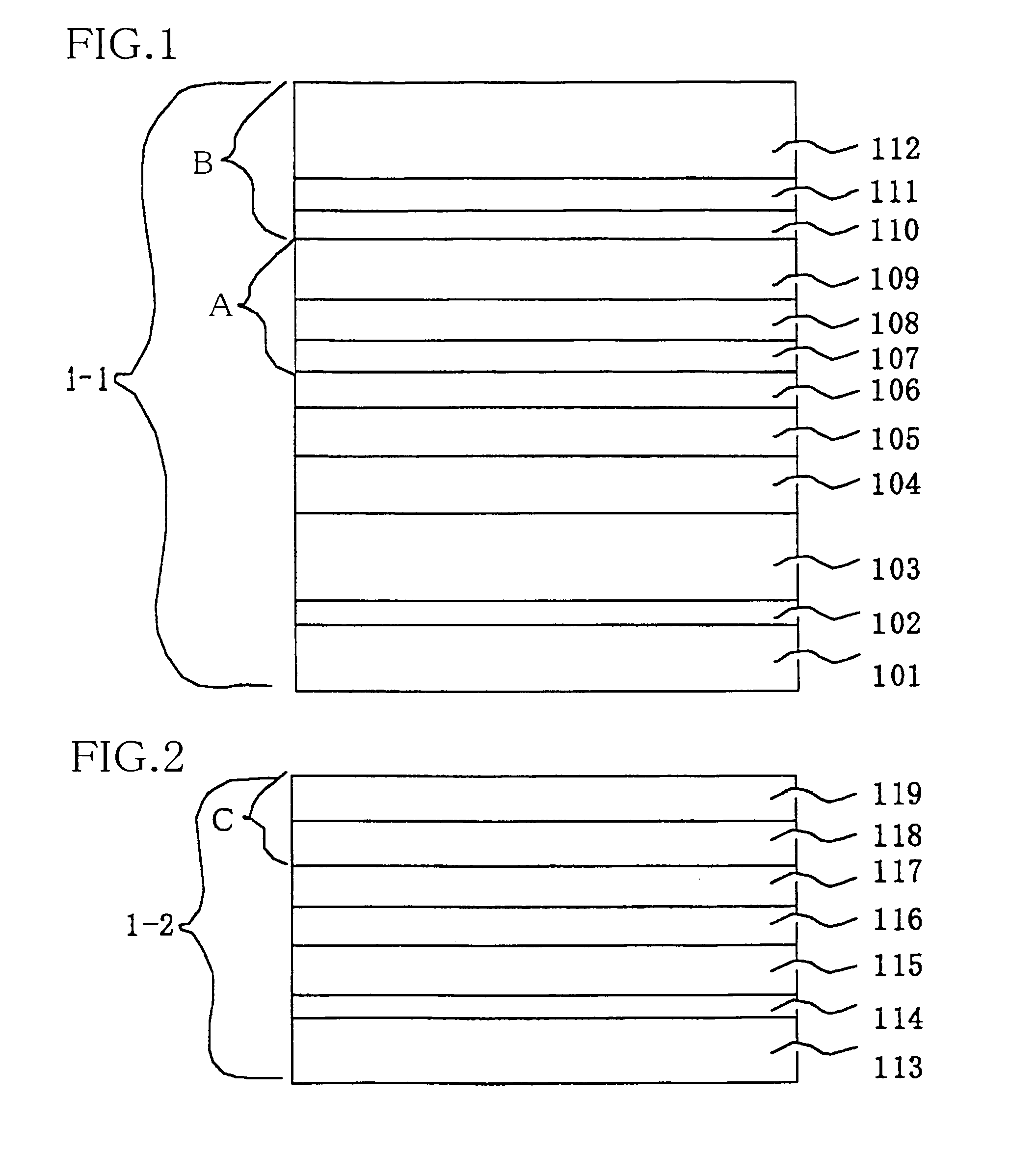
[0030]FIG. 3 shows, in schematic cross section, a light emitting device of III group nitride semiconductor according to a first embodiment of the present invention. In this light emitting device, a transparent n-electrode 120 is formed on a lower surface of a stack 1-1 including a plurality of III group nitride semiconductor layers including a light emitting layer. Bonded on a multiple metal bonding-layer B at the upper side of stack 1-1 is a conductive substrate electrode 1-2 which includes a multiple metal bonding-layer C. Multiple metal bonding-layers B and C are bonded to each other.
[0031]To produce the light emitting device of FIG. 3, firstly, stack 1-1 as shown in FIG. 1 is fabricated. In fabrication of stack 1-1, a GaN buffer layer 102, an n-type GaN layer 103, a MQW (multiple quantum well) active layer 104 as a light emitting layer of four pairs of In0.08Ga0.92N sub-layers and GaN sub-layer stacked alternately, a p-type AlGaN layer 105, and a p-type GaN layer 106 are formed ...
second embodiment
[0047]FIG. 6 shows, in schematic cross section, a light emitting device of III group nitride semiconductor according to a second embodiment of the present invention. In this light emitting device, a transparent n-electrode 120 is formed on the lower surface of a stack 4-1 including a plurality of III group nitride semiconductor layers including a light emitting layer. A conductive substrate electrode 4-2 is bonded to a multiple metal bonding-layer E at the upper side of stack 4-1. Conductive substrate electrode 4-2 includes a multiple metal bonding-layer F, and then multiple metal bonding-layers E and F are bonded to each other.
[0048]To obtain the light emitting device of FIG. 6, firstly, stack 4-1 as shown in FIG. 4 is fabricated. In fabrication of stack 4-1, an AlN intermediate layer 402, an n-type GaN layer 403, an MQW active layer 404 as a light emitting layer formed of four pairs of In0.08Ga0.92N sub-layers and GaN sub-layers stacked alternately, a p-type AlGaN layer 405, and a...
third embodiment
[0058]A light emitting device of III group nitride semiconductor according to a third embodiment of the present invention has a structure similar to those of the first and second embodiments, and thus it can be fabricated with the steps similar to those for the first and second embodiments. In the third embodiment, however, ITO layer 108 or 408 in the first or second embodiment is doped with an impurity (La2O2S:Eu3+) causing a fluorescent effect. As a result, light externally extracted from the light emitting device of the III group nitride semiconductor can be converted to white light. Further, by controlling the thickness of ITO layer 108 or 408, effects similar to those in the first and second embodiments can also be obtained.
[0059]Moreover, in the third embodiment, for the impurity causing the fluorescent effect to be added to the ITO layer, at least one of (YAG:Ce), (La2O2S:Eu3+), (Y2O2S:Eu), (ZnS:Cu, Al) and ((Ba, Mg) Al10O17:Eu) may be employed to obtain the similar effect.
[0...
PUM
| Property | Measurement | Unit |
|---|---|---|
| thickness | aaaaa | aaaaa |
| thickness | aaaaa | aaaaa |
| wavelength range | aaaaa | aaaaa |
Abstract
Description
Claims
Application Information
 - R&D
- Intellectual Property
- Life Sciences
- Materials
- Tech Scout
- Unparalleled Data Quality
- Higher Quality Content
- 60% Fewer Hallucinations
Browse by: Latest US Patents, China's latest patents, Technical Efficacy Thesaurus, Application Domain, Technology Topic, Popular Technical Reports.
© 2025 PatSnap. All rights reserved.Legal|Privacy policy|Modern Slavery Act Transparency Statement|Sitemap|About US| Contact US: help@patsnap.com