Nitride gallium compound semiconductor light emission device
a technology of gallium compound and light emission device, which is applied in the direction of semiconductor devices, electrical equipment, basic electric elements, etc., can solve the problems of reducing the amount of light generated by the light emission device and the total light output power obtained from the light emission devi
- Summary
- Abstract
- Description
- Claims
- Application Information
AI Technical Summary
Benefits of technology
Problems solved by technology
Method used
Image

Examples
example 1
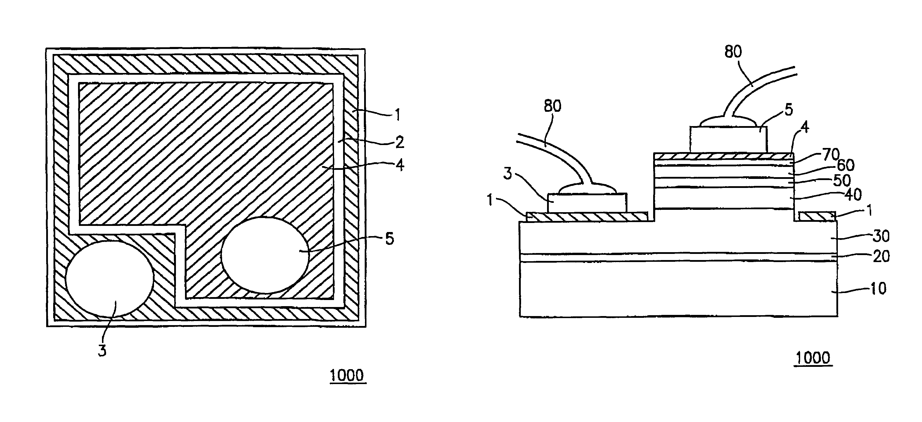
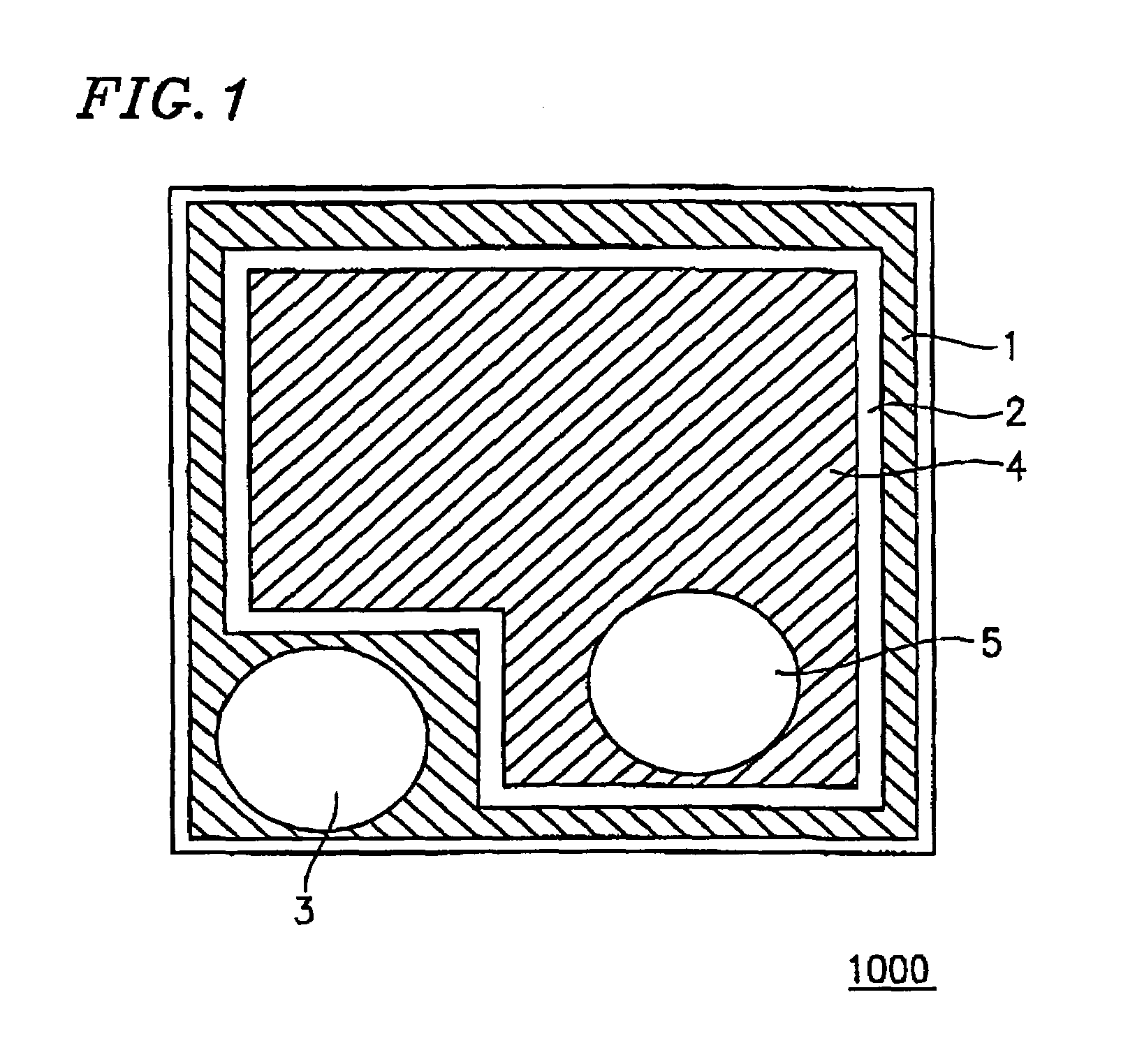
[0039]FIG. 1 is a schematic plan view illustrating a light emission device 1000 according to Example 1 of the present invention. The light emission device 1000 includes a GaN compound semiconductor multilayer structure including at least a light emission layer (active layer). The GaN compound semiconductor multilayer structure generally includes p-type GaN compound semiconductor layers and n-type GaN compound semiconductor layers. Upon one of the p-type GaN compound semiconductor layers, a p-type transmissive electrode 4 and a p-type pad electrode 5 are formed (the p-type transmissive electrode 4 and a p-type pad electrode 5 may collectively be referred to as a “p-type electrode region”). Upon one of the n-type GaN compound semiconductor layers, an n-type transmissive electrode 1 is formed around the circumference of the p-type transmissive electrode 4. An n-type pad electrode 3 is formed on the n-type transmissive electrode 1 (the n-type pad electrode 3 and the n-type transmissive ...
example 2
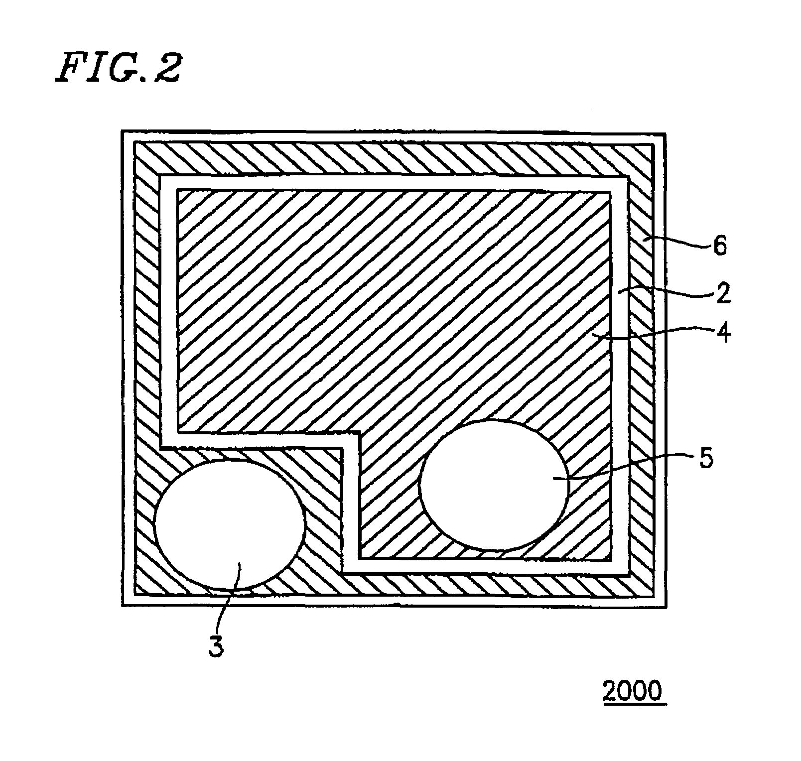
[0053]FIG. 2 is a schematic plan view illustrating a light emission device 2000 according to Example 2 of the present invention. The light emission device 2000 includes a GaN compound semiconductor multilayer structure including at least a light emission layer (active layer). The GaN compound semiconductor multilayer structure generally includes p-type GaN compound semiconductor layers and n-type GaN compound semiconductor layers. Upon one of the p-type GaN compound semiconductor layers, a p-type transmissive electrode 4 and a p-type pad electrode 5 are formed. Upon one of the n-type GaN compound semiconductor layers, an n-type transmissive electrode 6 is formed around the circumference of the p-type transmissive electrode 4. The n-type transmissive electrode 6 has a double-layer structure including a transmissive thin metal film and an oxide semiconductor layer. An n-type pad electrode 3 is formed on the n-type transmissive electrode 6.
[0054]The production method and construction o...
example 3
[0057]FIG. 3 is a schematic plan view illustrating a light emission device 3000 according to Example 3 of the present invention. The light emission device 3000 includes a GaN compound semiconductor multilayer structure including at least a light emission layer (active layer). The GaN compound semiconductor multilayer structure generally includes p-type GaN compound semiconductor layers and n-type GaN compound semiconductor layers. Upon one of the p-type GaN compound semiconductor layers, a p-type transmissive electrode 4 and a p-type pad electrode 5 are formed. An n-type transmissive electrode 1 is formed around the circumference of the p-type transmissive electrode 4. No electrode is formed in a region 2.
[0058]Next, a method for producing the light emission device 3000 according to the present example will be specifically described with reference to FIGS. 9A to 9E.
[0059]First, a GaN compound semiconductor multilayer structure is formed on a conductive GaN substrate 10 by using an M...
PUM
 Abstract
Description
Claims
Application Information
 - R&D
- Intellectual Property
- Life Sciences
- Materials
- Tech Scout
- Unparalleled Data Quality
- Higher Quality Content
- 60% Fewer Hallucinations
Browse by: Latest US Patents, China's latest patents, Technical Efficacy Thesaurus, Application Domain, Technology Topic, Popular Technical Reports.
© 2025 PatSnap. All rights reserved.Legal|Privacy policy|Modern Slavery Act Transparency Statement|Sitemap|About US| Contact US: help@patsnap.com