
Arithmetic built-in self-test of multiple scan-based integrated circuits

a built-in, integrated circuit technology, applied in error detection/correction, emergency protective circuit arrangements, instruments, etc., can solve problems such as excessive delays, increase latency, and compromise of ic's area and performance, and achieve the effect of reducing the impact of an error compensation phenomenon

Inactive Publication Date: 2005-10-11
MENTOR GRAPHICS CORP
View PDF23 Cites 36 Cited by
  • Summary
  • Abstract
  • Description
  • Claims
  • Application Information

AI Technical Summary

Benefits of technology

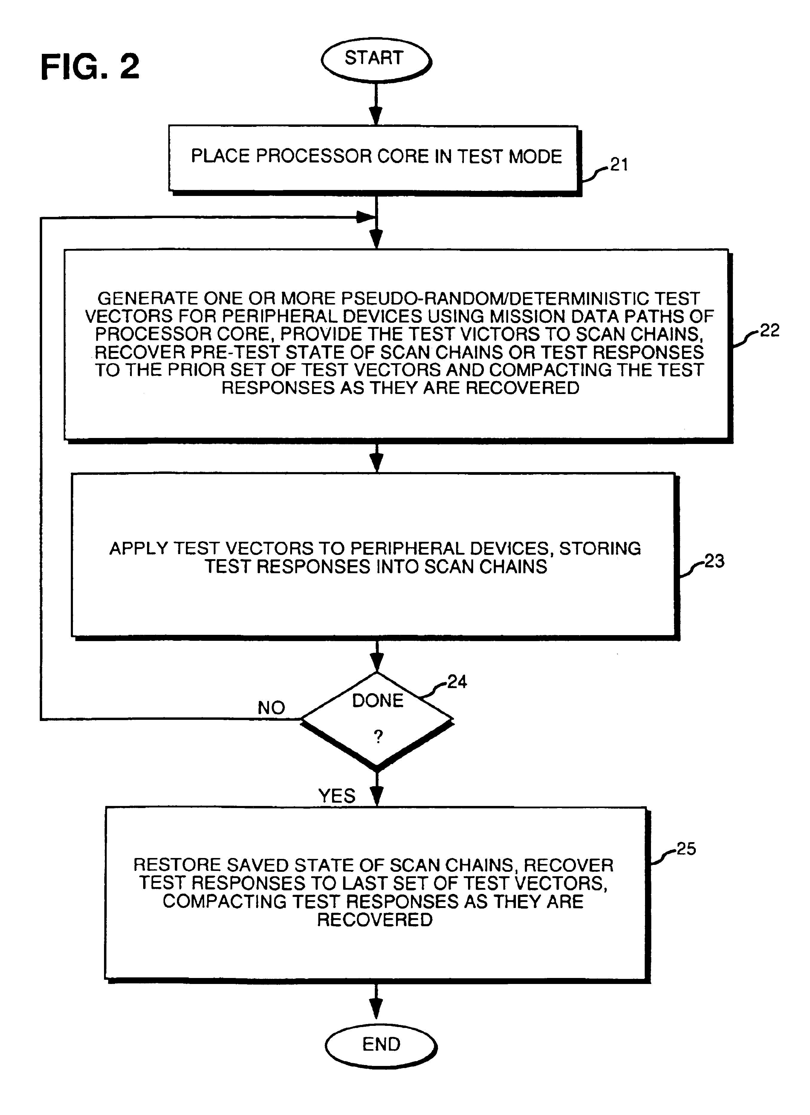
[0017]In accordance with yet another aspect of the present invention, the IC is further provided with microcode that implements an arithmetic test response compactor, which when executed by the embedded processor core, compacts test responses of the peripheral devices into a signature. The arithmetic test response compactor compacts the test responses in a cascaded add-and-accumulate manner, reducing the impact of an error compensation phenomenon.

Problems solved by technology

However, this solution compromises an IC's area and performance as it inevitably introduces either a hardware overhead or additional delays and increased latency.
These delays may be excessive for high-speed ICs used in several applications such as high-performance microprocessors, digital signal processing (DSP) systems, new generations of floating point processors, and others.
The solutions range from pseudo-random techniques that do not use any storage (for test data) but take a long application time and often do not detect some faults to deterministic techniques that may require significant storage but achieve complete fault coverage in a relatively short time.
A common drawback of the scan-path techniques is a long test application time due to the need to scan data in and out of the circuit.
146-152, and, due to structural and linear dependencies, may not be able to produce some test patterns.
In general, schemes based on pseudo-random patterns may fail to detect some faults in some circuits due to inherent limitations of pseudo-random test vectors.
This approach rests on the fact that the deterministic test patterns frequently feature a large number of unspecified positions.
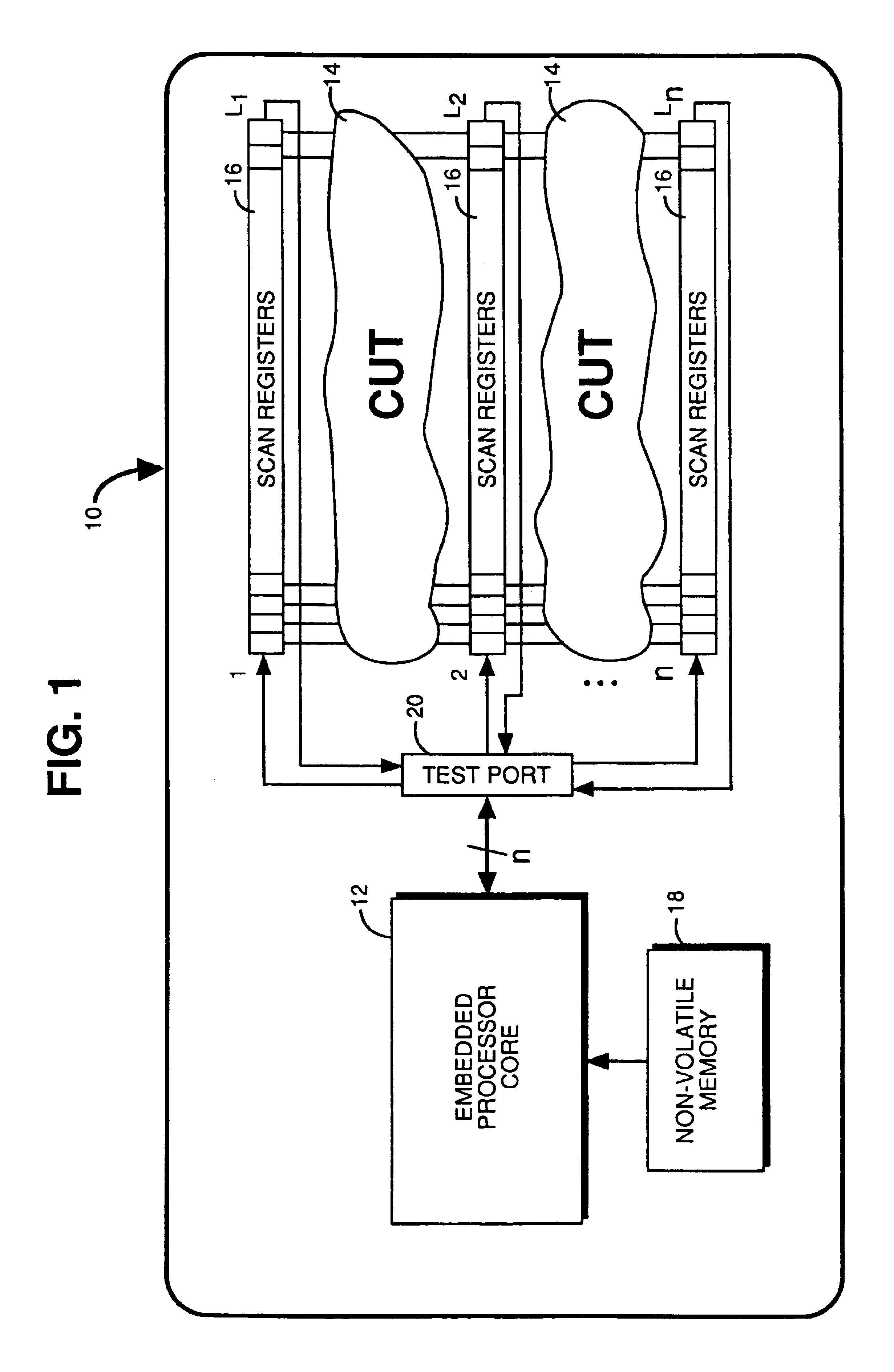
However, the ABIST proposal presented in the Adham article did not address generation of test patterns for peripheral devices, in particular, peripheral devices with “shortened” multiple scan-chains in ICs.

Method used


Image

  • Arithmetic built-in self-test of multiple scan-based integrated circuits
  • Arithmetic built-in self-test of multiple scan-based integrated circuits
  • Arithmetic built-in self-test of multiple scan-based integrated circuits

Examples


Embodiment Construction

[0028]In the following description, various aspects of the present invention will be described. However, it will be apparent to those skilled in the art that the present invention may be practiced with only some or all aspects of the present invention. For purposes of explanation, specific numbers, materials and configurations are set forth in order to provide a thorough understanding of the present invention. However, it will also be apparent to one skilled in the art that the present invention may be practiced without the specific details. In other instances, well known features are omitted or simplified for clarity.

[0029]Parts of the description will be presented in terms of operations performed inside an integrated circuit with an embedded processor core and peripheral devices, using terms such as data, bits, values, numbers and the like, consistent with the manner commonly employed by those skilled in the art to convey the substance of their work to others skilled in the art. A...


PUM


Abstract

An apparatus and method provide for an arithmetic built-in self test (ABIST) of a number of peripheral devices having parallel scan registers coupled to a processor core, all within an integrated circuit. Using the data paths of the processor core, operating logic generates pseudo-random test patterns for the peripheral devices, employing a mixed congruential generation scheme. In one embodiment, generating the pseudo-random test patterns includes multiplying n least significant bits of a 2n-bit pseudo-random number generated in an immediately preceding iteration and stored in a first register, with an n-bit multiplier constant stored in a second register to produce a 2n-bit product, adding the 2n-bit product to n most significant bits of the 2n-bit pseudo-random number stored in n least significant locations of an accumulator with 2n locations to produce a new 2n-bit pseudo-random number for a current iteration, and outputting n least significant bits of the new 2n-bit pseudo-random number as an n-bit pseudo-random test vector for the peripheral devices.

Description

CROSS-REFERENCE TO PRIOR APPLICATIONS[0001]This application is a continuation of U.S. patent application Ser. No. 09 / 276,474, filed Mar. 25, 1999, which is a continuation of U.S. patent application Ser. No. 08 / 814,042, filed on Mar. 10, 1997, now U.S. Pat. No. 5,991,898, issued Nov. 23, 1999, both of which are hereby incorporated by reference.BACKGROUND OF THE INVENTION[0002]1. Field of the Invention[0003]The present invention relates generally to testing of integrated circuits (IC) and more particularly to arithmetic built-in self-test (ABIST) of multiple scan-based ICs.[0004]2. Background Information[0005]Many ICs are produced in large volume and very often operate at high speeds. Since their manufacturing yield strongly depends on the silicon area, and their performance is directly related to the delays on critical paths, it is essential that the testing strategy provides a high fault coverage without a significant area overhead and performance degradation. As the costs associate...

Claims


Application Information

Patent Timeline
Patent Type & Authority Patents(United States)
IPC IPC(8): G01R31/3185G01R31/28G06F11/267
CPCG01R31/318385G01R31/318547G06F11/2221
Inventor RAJSKI, JANUSZTYSZER, JERZY
Owner MENTOR GRAPHICS CORP
Learn More