Multi-domain liquid crystal display device

Inactive Publication Date: 2005-09-06
LG DISPLAY CO LTD
View PDF27 Cites 13 Cited by
  • Summary
  • Abstract
  • Description
  • Claims
  • Application Information

AI Technical Summary

Benefits of technology

[0016]An object of the present invention is to provide a multi-domain LCD having high response time characteristics and high brightness by stable arrangement of liquid crystal molecules.

Problems solved by technology

If the electrodes do not have an open area or the width of the open area is narrow, the electric field distortion needed to divide the pixel region becomes weak.
At this time, disclination occurs from the area where the liquid crystal directors are parallel with a transmittance axis of the polarizer, which results in a decrease in brightness.

Method used


Image

  • Multi-domain liquid crystal display device
  • Multi-domain liquid crystal display device
  • Multi-domain liquid crystal display device

Examples


first embodiment

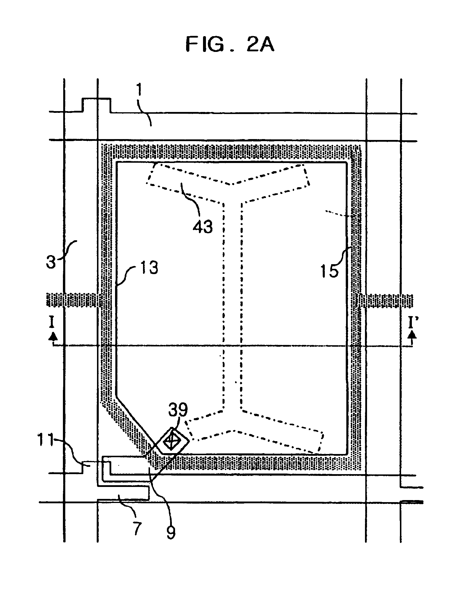
[0031]FIGS. 2A, 2B, 2C, 2D, 2E, 2F, and 2G are plan views of the multi-domain liquid crystal display device according to the present invention, FIGS. 2H, 2I are sectional views taken along the lines I-I′ of FIG. 2A, and FIGS. 2J, 2K are entire sectional views according to the FIG. 2H.

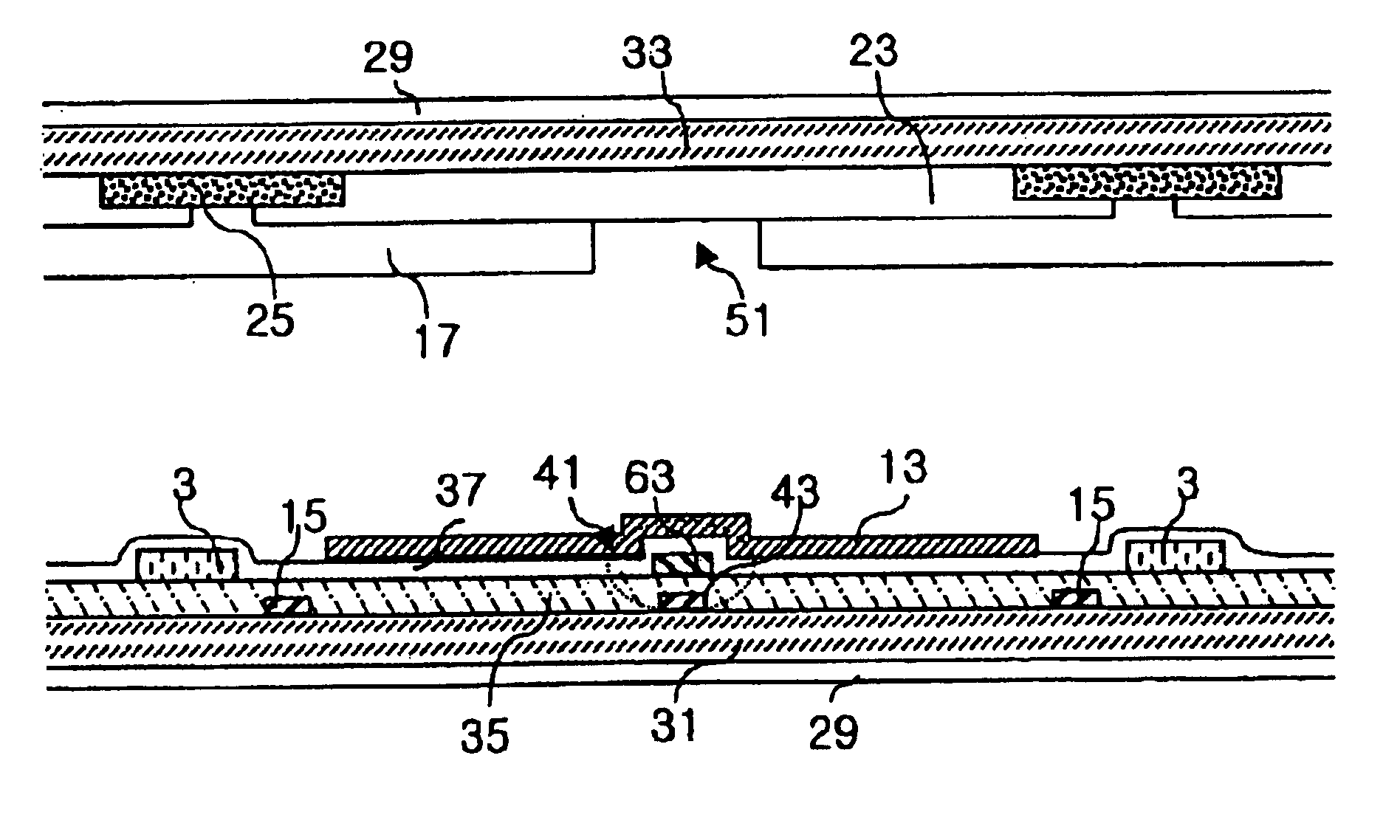
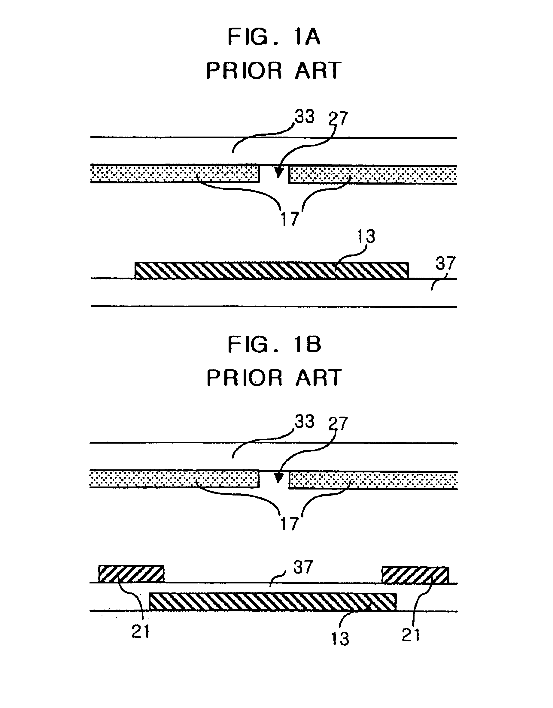
[0032]As shown in the figures, the present invention comprises first and second substrates 31, 33, a plurality of gate bus lines 1 arranged in a first direction on the first substrate and a plurality of data bus lines 3 arranged in a second direction on the first substrate, a TFT, a passivation layer 37, a pixel electrode 13, and a common-auxiliary electrode 15.

[0033]Data bus lines 3 and gate bus lines 1 divide the first substrate 31 into a plurality of pixel regions. The common-auxiliary electrode 15 distorts electric field on a same layer whereon the pixel electrode 13 is formed. The TFT is formed on each pixel region and comprises a gate electrode 11, a gate insulator 35, a semiconductor layer, an oh...

second embodiment

[0041]FIGS. 3A, 3B, 3C, 3D, 3E, 3F, and 3G are plan views of the multi-domain liquid crystal display device according to the present invention, FIG. 3H is sectional view taken along the lines II-II′ of FIG. 3A, and FIGS. 3I, 3J are entire sectional views according to the FIG. 3H.

[0042]As shown in the figures, the present invention comprises first and second substrates 31, 33, a plurality of gate bus lines 1 arranged in a first direction on the first substrate 31 and a plurality of data bus lines 3 arranged in a second direction on the first substrate 31, a common-auxiliary electrode 15, a first storage electrode 43, a TFT, a passivation layer 37, and a pixel electrode 13.

[0043]Data bus lines 3 and gate bus lines 1 divide the first substrate 31 into a plurality of pixel regions. The first storage electrode 43 is in the pixel region and on a same layer whereon the gate bus line 1 is formed, and is connected to or independently formed with the common-auxiliary electrode 15 to make a st...


PUM


Abstract

A multi-domain liquid crystal display device includes first and second substrates facing each other and a liquid crystal layer between the first and second substrates. A conductive layer distorting electric field is on the first substrate, and a common-auxiliary electrode is on a same layer whereon the conductive layer distorting electric field is formed. A common electrode is on the second substrate, and a storage electrode is in an electric field inducing region that divides the liquid crystal layer into at least two domains.

Description

CROSS-REFERENCE TO RELATED APPLICATIONS[0001]This application is a divisional application of patent application Ser. No.: 09 / 497,507, filed Feb. 4, 2000 now U.S. Pat. No. 6,680,769, now allowed; which claims priority to Korean Patent Application No.: P1999-4195, filed Feb. 8, 1999 and Korean Patent Application No.: P1999-14492, filed Apr. 22, 1999, all of which are incorporated by reference for all purposes as if fully set forth herein.BACKGROUND OF THE INVENTION[0002]1. Field of the Invention[0003]The present invention relates to a liquid crystal display device (LCD), and more particularly, to a liquid crystal display device having common-auxiliary electrodes surrounding pixel region and storage electrode in the pixel region.[0004]2. Description of the Related Art[0005]Recently, an LCD has been proposed where the liquid crystal is not aligned and the liquid crystal is driven by side electrodes insulated from pixel electrodes. FIGS. 1a and 1b are sectional views of pixel unit of the...

Claims


Application Information

Patent Timeline
IPC IPC(8): G02F1/13G02F1/1333G02F1/139G02F1/1362G02F1/136G02F1/1337G02F1/1343
CPCG02F1/133707G02F1/136213G02F1/1393G02F1/1337G02F1/1343G02F1/136
Inventor LEE, YUN BOKKO, DOO HYUNLEE, JOUN HO
Owner LG DISPLAY CO LTD
Why Eureka
Try Eureka