
Sensors and probes for mapping electromagnetic fields

a technology of electromagnetic field and electromagnetic field, applied in the field of measuring and testing electricity, can solve the problems of electromagnetic field, electromagnetic field, etc., and achieve the effects of reducing the complexity of analysis, reducing the difficulty of detecting and mapping electromagnetic field vectors, and reducing the complexity of electromagnetic field vectors

Inactive Publication Date: 2005-08-23
ALBANY INSTR
View PDF8 Cites 79 Cited by
  • Summary
  • Abstract
  • Description
  • Claims
  • Application Information

AI Technical Summary

Benefits of technology

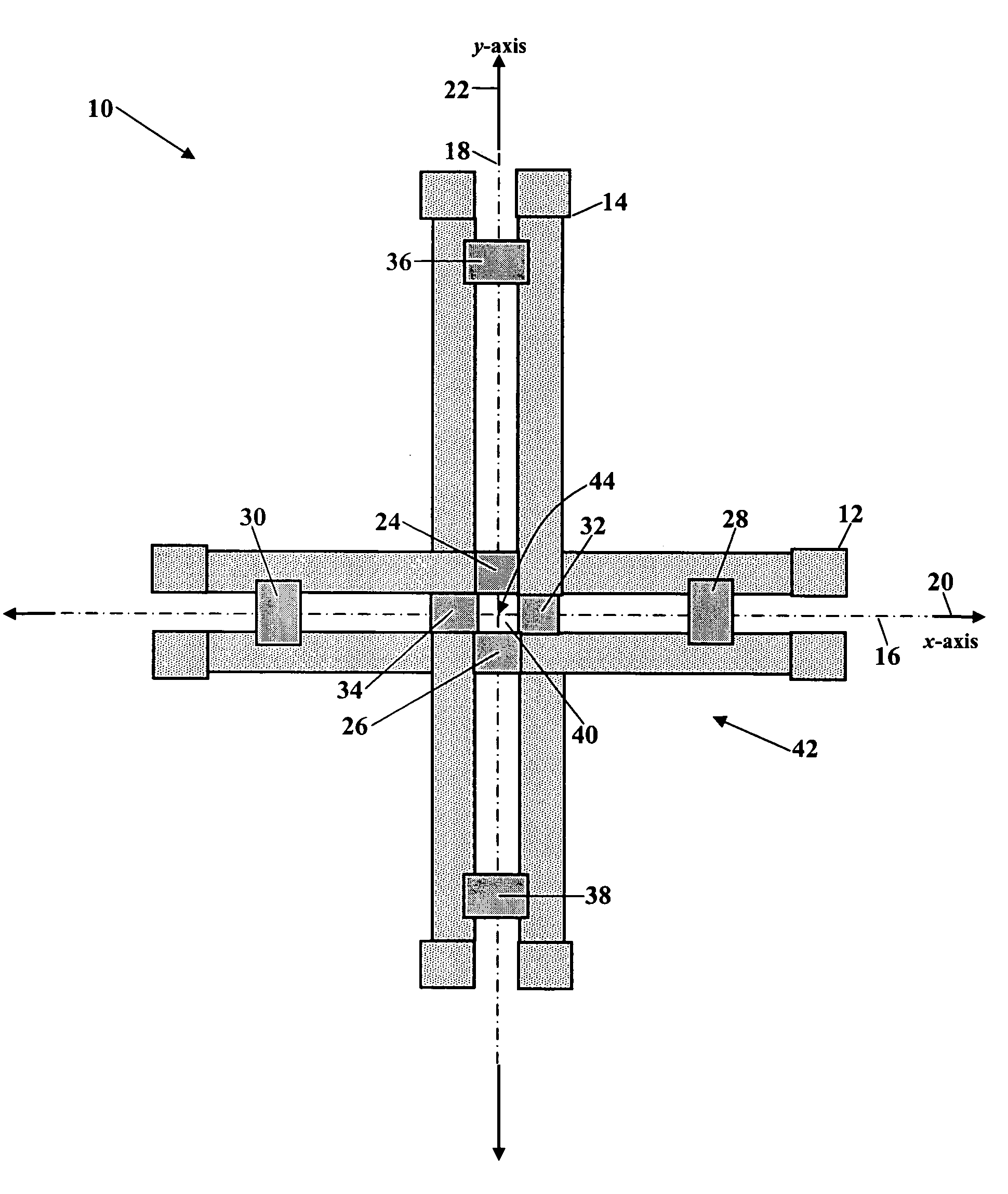
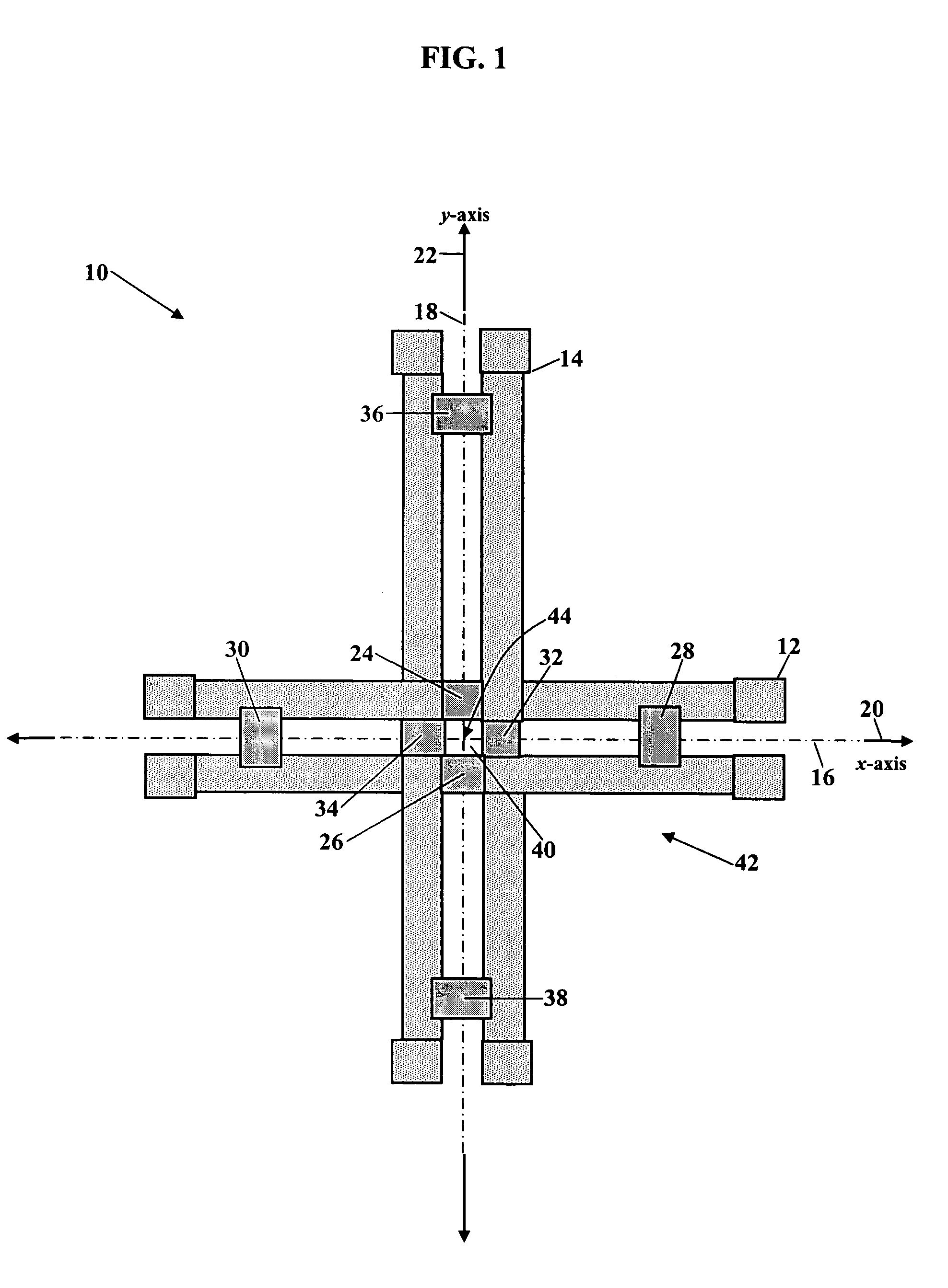
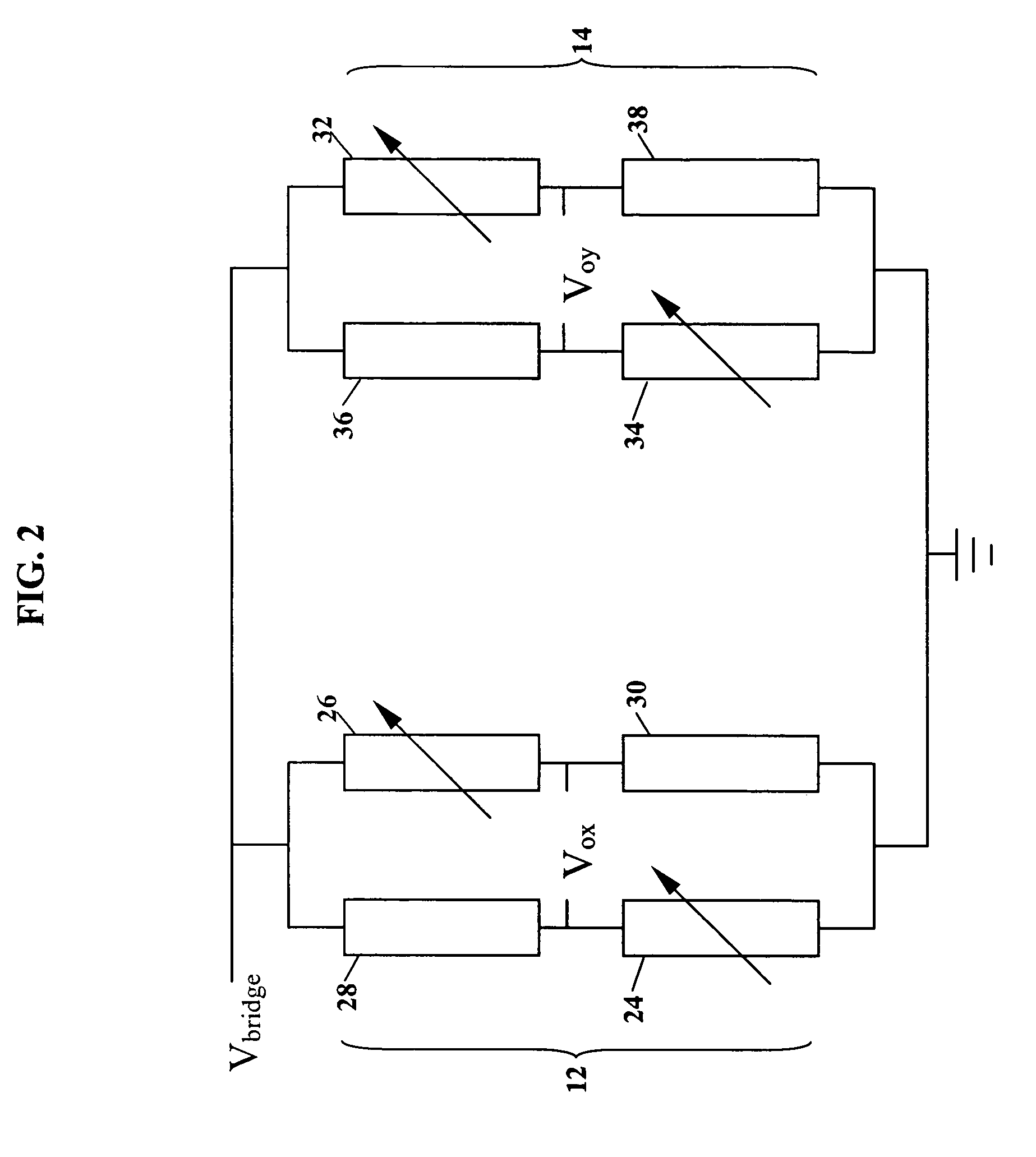
[0009]The aforementioned problems are reduced by sensors of the present invention. A sensor according to the present invention is able to isolate individual vector components of electromagnetic fields. Sensors of the present invention measure two components of an electromagnetic field within a plane, essentially at the same point. Sensors of the present invention may also be arranged to measure three components of an electromagnetic field within a localized area about a central point. Because these sensors may have a small sensitive area, these sensors permit high-resolution electromagnetic field mapping. Sensors of the present invention may also be manufactured using planar technology, further permitting integrated sensor arrays for mapping fields without the need to scan test specimens. These sensors also allow the design of eddy current probes, and arrays of probes, for nondestructive testing and metallic profilometry, thus permitting new methods of detection of defects using these probes and arrays of probes.
[0010]One embodiment, for example, is substantially only sensitive in one direction. This embodiment has little to no response to electromagnetic fields in directions other than this single, sensitive direction. Sensors of the present invention, therefore, yield much more precise measurements of electromagnetic fields. Sensors of the present invention also exhibits a linear response and constant sensitivity over a wide range of frequencies, from DC to the megahertz domain. Because such sensors may be manufactured on silicon substrates, embodiments may be very small with high spatial resolution. Silicon substrate technology also allows many sensors to be manufactured on a single wafer. Sensors of the present invention are, therefore, small, precise, and inexpensive.
[0019]Still another embodiment discloses a product for mapping flaws in specimens. A coil induces an electromagnetic field in the specimen. A first magneto-resistive sensor and a second magneto-resistive sensor have a coplanar relationship and are orthogonally arranged. The first magneto-resistive sensor measures the induced electromagnetic field along a first sensitive axis in the plane. The second magneto-resistive sensor measures the induced electromagnetic field along a second sensitive axis in the plane. The first and second magneto-resistive sensors measure orthogonal components of the induced electromagnetic field in an area of the central point. A perpendicular sensor measures perturbations in the induced electromagnetic field in a direction perpendicular to the plane of the at least two coplanar magneto-resistive sensors. The flaw creates a perturbation in the induced electromagnetic field, and the orthogonal arrangement of the first and second magneto-resistive sensors detects orthogonal components of this perturbation, and the orthogonal components map the flaw. The product, having the first and the second magneto-resistive sensors, enables the mapping of a randomly-oriented crack or determining the orientation of a crack having an unknown orientation.

Problems solved by technology

The mapping of electromagnetic field vectors is extremely difficult and complex.
Electromagnetic fields, however, are often extremely complex to mathematically describe.
This analysis is considerably complicated when the line, surface, or volume is complexly shaped and cannot be described using mathematics.
There are, however, several problems with existing electromagnetic sensors.
Although the prior art sensors may be designed to measure electromagnetic fields in one dimension, the prior art sensors are still sensitive to electromagnetic field vector components in other dimensions.
Another problem is frequency dependence of existing inductive sensors.
Many existing inductive sensors only have an adequate output over a preferred frequency range.
If the frequency of the electromagnetic field lies outside the preferred frequency range, the sensitivity of existing inductive sensors are greatly reduced and measurements are lost or compromised.
Thus, although sensors are often used to measure complex electromagnetic fields, these problems with existing sensor designs still present limitations in the measurement of electromagnetic fields.

Method used


Image

  • Sensors and probes for mapping electromagnetic fields
  • Sensors and probes for mapping electromagnetic fields
  • Sensors and probes for mapping electromagnetic fields

Examples


examples

[0075]The sensors of the present invention are further illustrated by the following non-limiting examples. These non-limiting examples describe various eddy current probes utilizing the sensors of the present invention. Eddy current probes are used to detect cracks in electrically conductive materials. An eddy current probe, more specifically, induces eddy currents in a specimen, and the probe detects perturbations in the induced eddy currents. The perturbations indicate a crack is present.

[0076]FIG. 14 is a schematic drawing of an eddy current probe 74. The probe 74 may comprise a flat, pancake-style coil 76 and any sensors shown in FIGS. 1–8. The probe 74, for simplicity, is shown comprising a solid-state sensor package 78. The sensor package 78 is shown containing the substrate 70, as shown in FIG. 13. At least one sensor 10 is shown formed on the substrate 70. The sensor package 78 is coaxially located along a coil axis 80 and adhesively bonded to the coil 76. The coil 76 has a ...


PUM


Abstract

Products are disclosed for measuring electromagnetic fields. One embodiment has at least two coplanar magneto-resistive sensors. Each magneto-resistive sensor has a sensitive axis in the plane of the at least two coplanar magneto-resistive sensors. The at least two magneto-resistive sensors may be orthogonally arranged about a central point to measure orthogonal components of electromagnetic fields.

Description

CROSS-REFERENCE TO RELATED APPLICATIONS[0001]This application is a divisional application of U.S. patent application Ser. No. 09 / 950,093 filed Sep. 10, 2001, now U.S. Pat. No. 6,822,443 which claims the benefit of the following applications: U.S. Provisional Application No. 60 / 231,752, filed Sep. 11, 2000; U.S. Provisional Application No. 60 / 247,245, filed Nov. 13, 2000; and U.S. Provisional Application No. 60 / 254,296, filed Dec. 11, 2000.NOTICE OF COPYRIGHT PROTECTION[0002]A portion of the disclosure of this patent document and its figures contain material subject to copyright protection. The copyright owner has no objection to the facsimile reproduction by anyone of the patent document or the patent disclosure, but otherwise reserves all copyrights whatsoever.BACKGROUND OF THE INVENTION[0003]1. Field of the Invention[0004]This invention generally relates to measuring and testing electricity and, more particularly, to sensors, to probes, and to arrays of probes and sensors for dete...

Claims


Application Information

Patent Timeline
IPC IPC(8): G01N27/90
CPCG01N27/904G01R33/093G01N27/902
Inventor DOGARU, TEODORSMITH, STUART T.
Owner ALBANY INSTR
Learn More