Film carrier tape for mounting an electronic part

a technology for electronic parts and film carriers, which is applied in the direction of magnetic materials, magnetic bodies, vehicle sealing arrangements, etc., can solve the problems of low productivity, large variability range of peel strength of gold wire thus bonded, and low peel strength, so as to improve the bonding strength and stabilize the bonding strength. , the effect of enhancing the bonding strength of gold wire to the surface layer containing gold as a main constituen

Inactive Publication Date: 2005-05-10
MITSUI MINING & SMELTING CO LTD
View PDF8 Cites 7 Cited by
  • Summary
  • Abstract
  • Description
  • Claims
  • Application Information

AI Technical Summary

Benefits of technology

[0012]It is an object of the present invention to provide a film carrier tape for mounting electronic part having high wire bonding strength, narrow variability of the strength, high bonding reliability, and high connection stability of solder ball disposed on the ball pad.
[0015]In the film carrier tape for mounting electronic part of the present invention, an extremely thin palladium layer having an average thickness of not more than 0.04 μm is formed between the undercoating layer containing nickel as a main constituent and the surface layer containing gold as a main constituent. Hence, the bonding strength of the gold wire to the surface layer containing gold as a main constituent is enhanced, and the bonding strength is stabilized. By the arrangement of such a thin intermediate layer of palladium, further, the solder ball placed on the ball pad is rarely influenced by the gold plated layer containing gold as a main constituent, and hence the solder ball can be stably disposed.

Problems solved by technology

In the production of the film carrier tape for mounting electronic part, however, the plated layer is generally formed as the undivided whole, and partial control of the thickness of the plated layer makes the production process complicated to thereby lower the productivity markedly.
However, it has been found that when the palladium plated layer of such thickness is interposed as an intermediate layer, then a gold plated layer is formed on the intermediate layer and a gold wire is bonded to the gold plated layer by the use of a bonding tool, variability range of the peel strength of the gold wire thus bonded becomes large.
However, the peel strength does not always become high, and besides the variability range of the peel strength tends to become large.
In the conventional film carriers, however, there is a fear of disconnection at the bonding pad (connecting terminal) having wide variability range of peel strength and low peel strength, even if the average peel strength in the wire bonding is not less than 8 gf.
Therefore, even if a palladium layer of large thickness is formed in accordance with the above-mentioned conventional technique, the variability range of the peel strength of the gold wire is increased, and the peel mode of B type or C type is liable to occur when the bonded wire is forcedly peeled.
Further, if the wire bonding strength is increased, the variability range of the peel strength of the solder ball becomes large, and it is impossible to improve both of those properties at the same time by the conventional technique.

Method used


Image

  • Film carrier tape for mounting an electronic part
  • Film carrier tape for mounting an electronic part
  • Film carrier tape for mounting an electronic part

Examples


example 1

Comparative Example 1

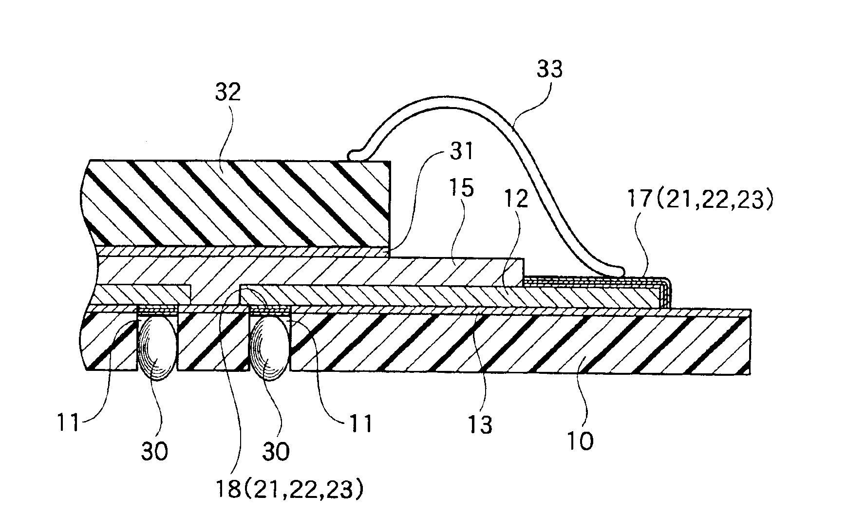
[0055]A polyimide film (available from Ube industries, Ltd., Upilex S) having a thickness of 50 μm was punched to form sprocket holes, solder ball holes, etc., and then to the film was laminated an electrodeposited copper foil having an average thickness of 25 μm by application of heat and pressure. Thereafter, the surface of the copper foil was coated with a photoresist. The resulting photoresist layer was subjected to light exposure and development in the conventional manner to form a desired pattern. Then, etching was carried out to form a desired wiring pattern.

[0056]The wiring pattern thus formed was coated with a solder resist, except the lead sections, and the solder resist was thermally cured.

[0057]Then, the lead (bonding pad (connecting terminal)) sections exposed from the solder resist layer formed as above and the ball pad sections exposed from the solder ball holes were subjected to acid washing to perform degreasing. Then, nickel plating was carried...

example 2

[0083]A film carrier tape was prepared in the same manner as in Example 1, except that the thickness of the palladium plated layer was changed to 0.002 μm and the thickness of the gold plated layer was changed to 0.50 μm. Then, various properties of the film carrier tape were measured in the same manner as in Example 1.

[0084]The results are set forth in Table 3.

example 3

[0088]A film carrier tape was prepared in the same manner as in Example 1, except that the thickness of the palladium plated layer was changed to 0.01 μm and the thickness of the gold plated layer was changed to 0.50 μm. Then, various properties of the film carrier tape were measured in the same manner as in Example 1.

[0089]The results are set forth in Table 4.


PUM

PropertyMeasurementUnit
thicknessaaaaaaaaaa
thicknessaaaaaaaaaa
thicknessaaaaaaaaaa

Abstract

A film carrier tape for mounting an electronic part comprising an insulating film and a wire pattern which is made of a conductive metal and is provided on the surface of the insulating film, wherein an undercoating layer containing nickel as a main constituent is formed on at least a part of the surface of the wiring pattern made of a conductive metal, an intermediate layer containing palladium as a main constituent is formed on the surface of he undercoating layer, a surface layer containing gold as a main constituent is formed on the surface of the intermediate layer, and the average thickness of the intermediate layer containing palladium as a main constituent is not more than 0.04 μm.

Description

BACKGROUND OF THE INVENTION[0001]The present invention relates to film carrier tapes for mounting electronic part, which have high reliability in the bonding of electronic parts to be mounted and whose outer connecting terminals, such as solder balls, also have high connection reliability. In the present invention, the film carrier tapes for mounting electronic part include those for TAB (tape automated bonding) method, COF (chip on film) method, CSP (chip size package) method, BGA (ball grid array) method, double-sided metal tape method, multi-layer wiring tape method, wire bonding method and flip chip bonding method.DESCRIPTION OF THE RELATED ART[0002]As methods to mount electronic parts such as IC on film carriers having wiring patterns formed thereon, there are known, for example, TAB (tape automated bonding) method, wire bonding method and flip chip bonding method. As the electronic parts have been more highly integrated and more densely mounted in recent years, film carrier ta...

Claims


Application Information

Patent Timeline
Patent Type & Authority Patents(United States)
IPC IPC(8): H01L23/48H01L23/498H05K3/24H05K1/00B32B15/08C25D7/00C25D5/12H01L21/60
CPCB32B15/08H01L23/4985H01L24/48H05K3/244H01L23/498Y10T428/12H01L2224/32225H01L2224/45015H01L2224/45144H01L2224/48091H01L2224/48227H01L2224/48472H01L2224/48599H01L2224/73265H01L2224/859H01L2924/01002H01L2924/01004H01L2924/01005H01L2924/01006H01L2924/01013H01L2924/01015H01L2924/01027H01L2924/01028H01L2924/01029H01L2924/01033H01L2924/01046H01L2924/01078H01L2924/01079H01L2924/01082H01L2924/01322H01L2924/014H01L2924/04953H01L2924/14H01L2924/15311H01L2924/20752H05K1/0393Y10T428/12201H01L2924/01019H01L24/45H01L2924/00014H01L2924/00012H01L2924/00H01L24/73H01L2224/85205H01L2224/85444H01L2224/85455H01L2224/85664
Inventor MATSUMURA, YASUNORIMAKITA, HIDEAKI
Owner MITSUI MINING & SMELTING CO LTD
Why Eureka
Try Eureka