Eureka AIR delivers breakthrough ideas for toughest innovation challenges, trusted by R&D personnel around the world.

Three layer aluminum deposition process for high aspect ratio CL contacts

a three-layer aluminum deposition and contact technology, applied in the field of dram fabrication, can solve the problems of destroying chucks, affecting the quality of dram,

Inactive Publication Date: 2004-09-21
POLARIS INNOVATIONS LTD
View PDF13 Cites 3 Cited by
  • Summary
  • Abstract
  • Description
  • Claims
  • Application Information

AI Technical Summary

Problems solved by technology

The cold-hot process is extremely slow and has a throughput of only about 22 wafers per hour for a two physical vapor deposition (PVD) Al chamber main frame.
The first or cold deposition suffers from the disadvantage of running unchucked, meaning that there is no opportunity to check whether the wafer is sitting correctly on the chuck that secures the wafer in a processing chamber.
If the wafer is not placed correctly on the chuck, the chuck may get deposited upon and ruined.
This is disadvantageous since an electrostatic chuck is very expensive.
A further problem with the conventional cold-hot process is the heat-up time needed in between the two Al depositions.
The conventional two-step deposition process is very slow due to the relatively long Al deposition time and a small amount of TiAl.sub.3 forms which increases contact resistance and decreases the electromigration lifetime.
Nevertheless, this two-step process is inadequate to fulfill the challenges needed due to the increasing aspect ratios that are necessary to make a void-free Al fill.

Method used


Image

  • Three layer aluminum deposition process for high aspect ratio CL contacts
  • Three layer aluminum deposition process for high aspect ratio CL contacts

Examples


Embodiment Construction

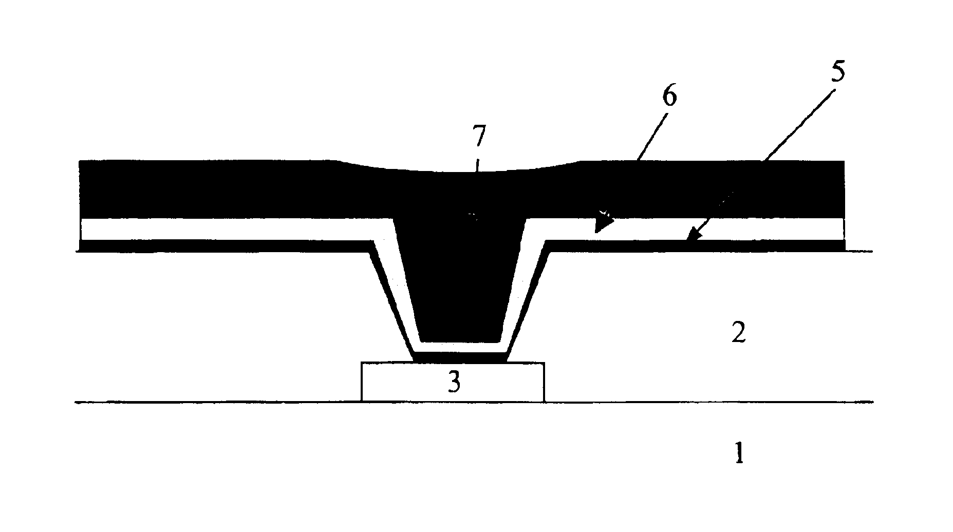
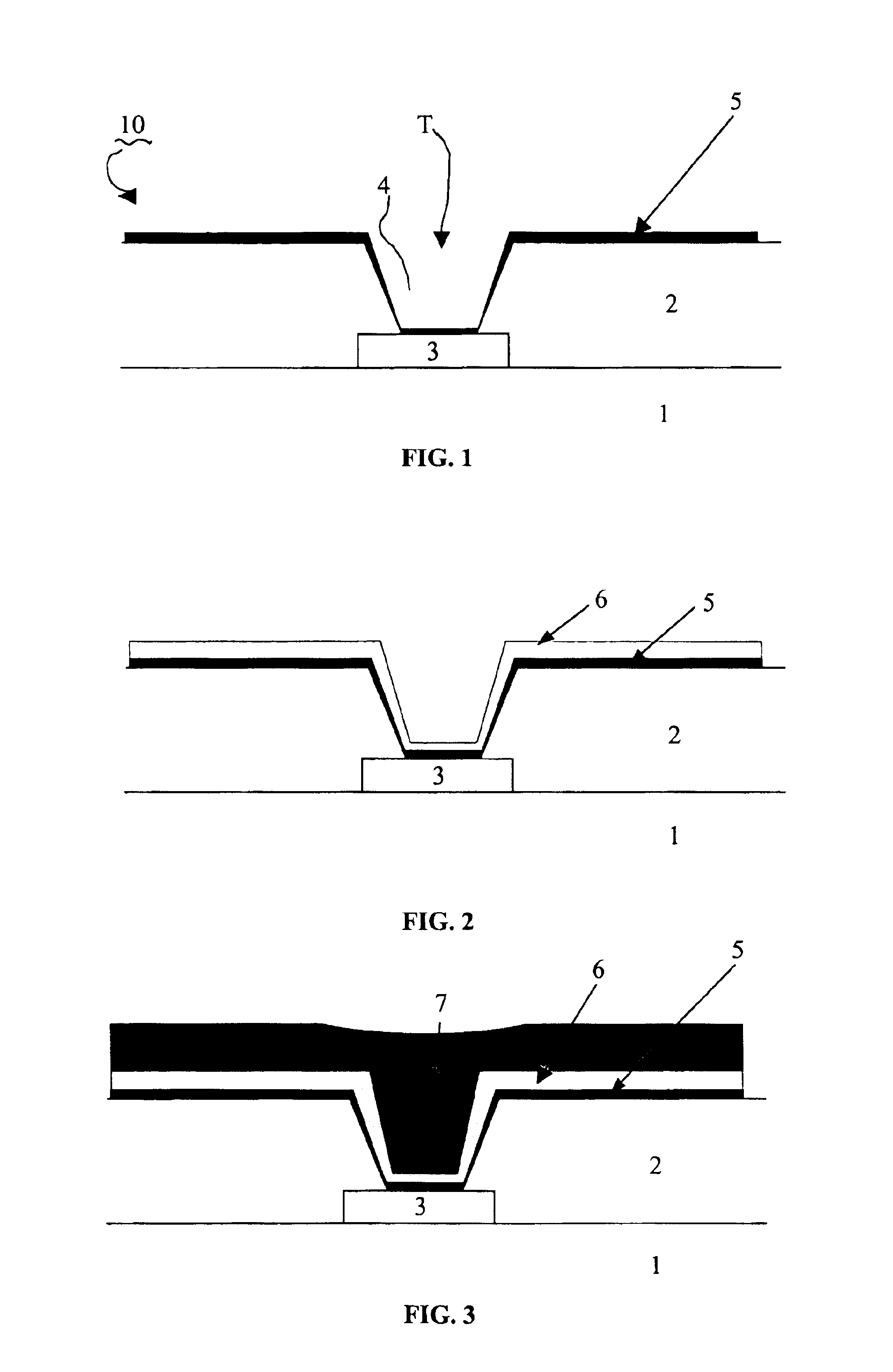
Reference is now made to FIG. 1 which is an illustrative depiction of a partial cross-sectional view of a semiconductor wafer 10. Wafer 10 includes a semiconductor memory chip, such as a dynamic random access memory (DRAM). The wafer as provided in the processing chamber (not shown) is at a stage such that it comprises a bottom layer of an intermetal dielectric 1 which preferably comprise SiO.sub.2 or a low-k -material. A target layer 2 is disposed on the bottom intermetal dielectric layer 1, and the target layer 2 comprises an intermetal dielectric, which is preferably SiO.sub.2 or a low-k -material. The target layer further includes a target conductor or metal layer 3 which is preferably composed of aluminum or copper which is a substrate having diffusion regions formed therein or conductive lines formed thereon. As may be seen from FIG. 1, the intermetal dielectric layer 2 is patterned to form a trench T and the trench may include contact holes or vias 4 and / or conductive line op...


PUM

PropertyMeasurementUnit
temperatureaaaaaaaaaa
thicknessaaaaaaaaaa
temperatureaaaaaaaaaa

Abstract

A method of forming a semiconductor device includes providing a semiconductor device including a conductor formed thereon. A dielectric layer is formed over the conductor and a recess is formed in the dielectric layer by removing a portion of the dielectric layer to expose at least a portion of the conductor. A first layer of aluminum is deposited over the top surface of the dielectric, along the sidewalls of the dielectric layer and over the exposed portion of the conductor without altering the temperature of the semiconductor device. A second layer of aluminum is deposited over the first layer of aluminum at a temperature greater than about 300° C. A third layer of aluminum is deposited over the second layer of aluminum so as to completely fill the recess in the dielectric layer. The third layer of aluminum is slow deposited at a temperature greater than about 300° C.

Description

1. Field of the InventionThe invention relates to DRAM fabrication and more particularly, to a process for forming a DRAM by utilizing a three layer aluminum deposition for contact levels (CL) for Al fill for the generation of 70 nm or 90 nm groundrule devices.2. Description of the Related ArtDRAM devices, such as semiconductor memories, processors, integrated circuits and the like, include layers of contact levels (CL) used to interconnect layers of metal. These conductive or metal lines (ML) are often formed on upper levels of a semiconductor device, and these metal lines are generally connected by contacts through vias to underlying devices or other metal lines.In the typical method, an Aluminum (Al) metal line deposition includes a two step process, and this process is a cold-hot process. The cold-hot process is extremely slow and has a throughput of only about 22 wafers per hour for a two physical vapor deposition (PVD) Al chamber main frame. The cold-hot process includes two d...

Claims


Application Information

Patent Timeline
Patent Type & Authority Patents(United States)
IPC IPC(8): H01L21/70H01L21/768H01L21/8242
CPCH01L21/76882H01L27/10888H01L21/2855H10B12/485
Inventor GOEBEL, THOMASROBL, WERNERMALIK, RAJEEVSEITZ, MIHEL
Owner POLARIS INNOVATIONS LTD
Why Eureka
Eureka Blog
Learn More