
Method and system for improving yield of semiconductor integrated circuits

a technology of integrated circuits and yields, applied in semiconductor/solid-state device testing/measurement, instruments, semiconductor devices, etc., can solve the problems of reducing the percentage yield per wafer, increasing the production yield, and involving several hundred or more operations

Inactive Publication Date: 2003-01-14
IBM CORP
View PDF6 Cites 34 Cited by
  • Summary
  • Abstract
  • Description
  • Claims
  • Application Information

AI Technical Summary

Problems solved by technology

Fabrication of semiconductor integrated circuits (IC's) is an extremely complex process that involves several hundred or more operations.
Increasing production yield is an ongoing challenge in the manufacture of semiconductor chips.
Because of various defects that can occur in the fabrication of a wafer, significant numbers of wafer die have to be discarded for one reason or another, thereby decreasing the percentage yield per wafer and driving up the cost of individual chips.
Defects are typically caused by foreign particles, minute scratches, and other imperfections introduced during photo-resist, photo-mask, etching, and diffusion operations.
Yield loss increases the number of wafer starts at the inception of production needed to meet specific customer order quantities for finished chips at the end of the production line and limits the number of good parts which can be sold.
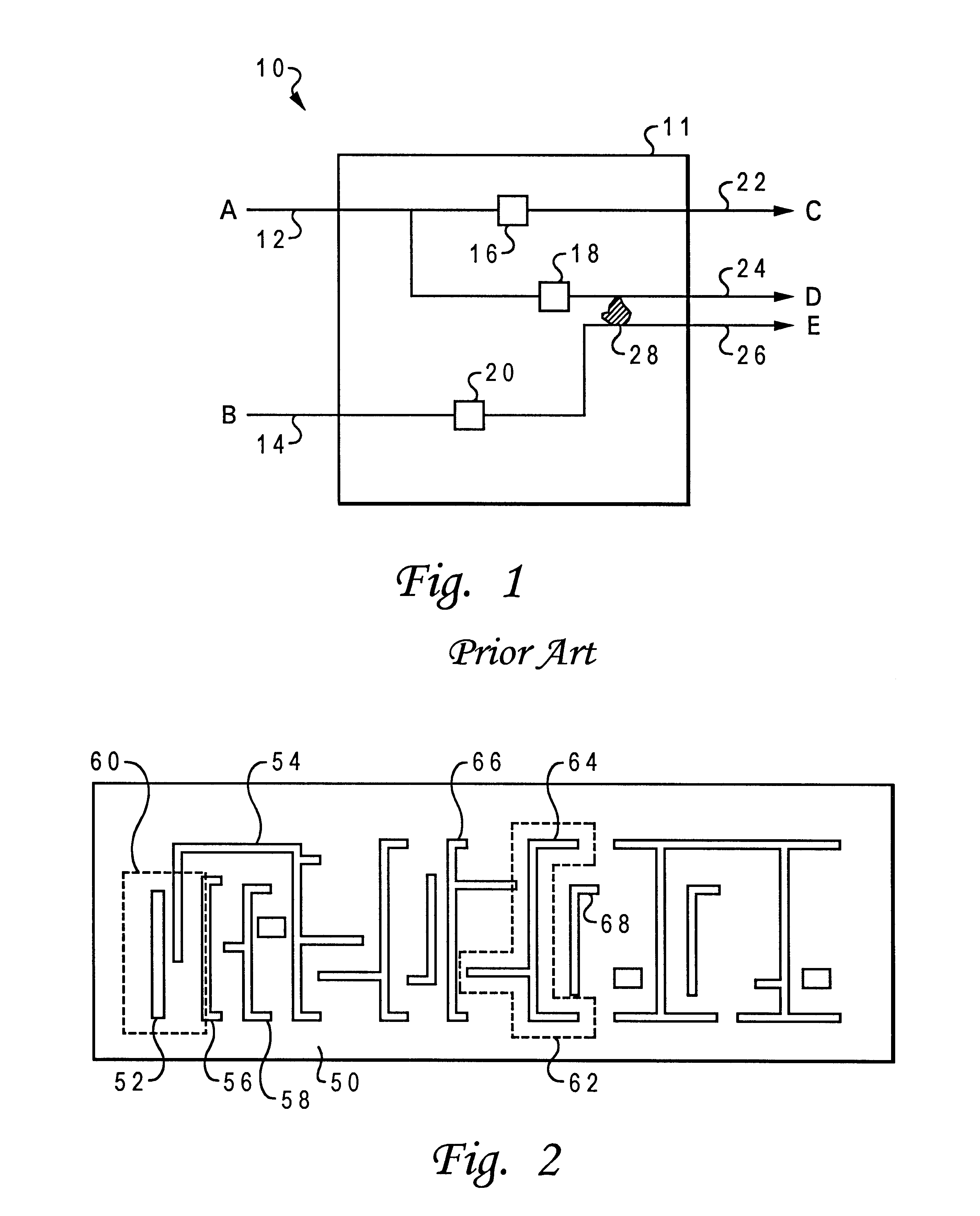
While design processes for automatic placement of conductive lines provide a minimum separation distance, they do not account for the general need to arrange the conductive lines in such a manner so that the areas which are especially susceptible to defects are minimized.
Because the minimum design rules do not account for areas which are especially susceptible to defects, the yield of usable devices produced from a wafer is not maximized.
Further, circuit layouts which are generated manually often may not be optimized for best yield.
Adherence to each of the set of rules throughout all of the layout reduces the yield.

Method used


Image

  • Method and system for improving yield of semiconductor integrated circuits
  • Method and system for improving yield of semiconductor integrated circuits
  • Method and system for improving yield of semiconductor integrated circuits

Examples


Embodiment Construction

A preferred embodiment of the present invention and its advantages are better understood by referring to FIGS. 1-5 of the drawings, like numerals being used for like and corresponding parts of the accompanying drawings.

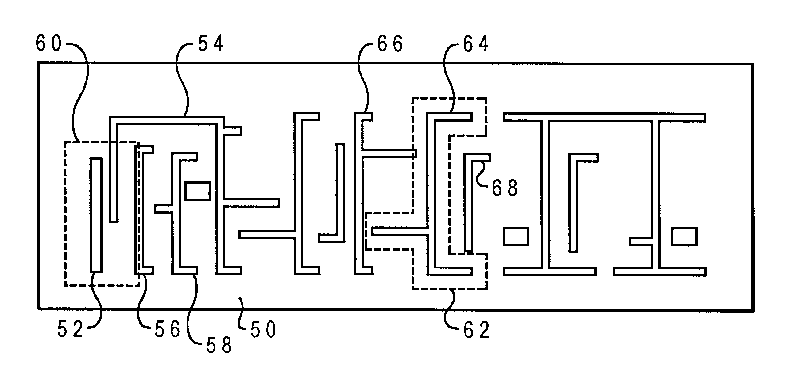
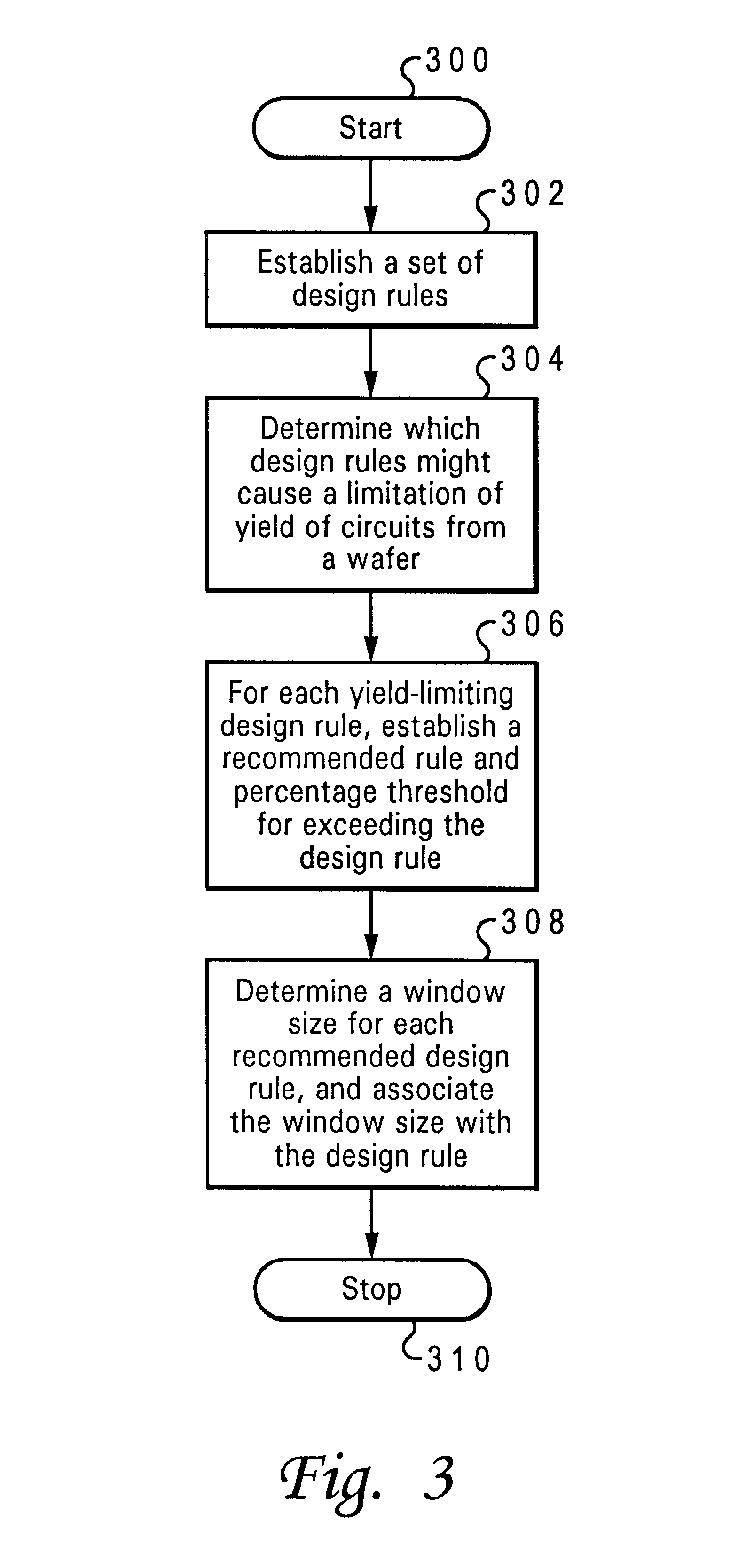
The present invention is a method and system for improving the yield of circuits produced from a semiconductor wafer by evaluating and enforcing compliance to a set of recommended design rules. Yield is maximized by requiring that recommended design rules be followed rather than the minimum design rules within the layout of the circuit wherever possible without adversely affecting the area of the circuit or performance.

For any given ground rule, there will be a minimum value. There may also be a value which is larger than the minimum value and which is known to improve yield if met, hereafter called the "recommended value" or "recommended design rule".

In general, there are several types of actions which will improve yield. Three types will be discussed relative to thi...


PUM


Abstract

A method and system are disclosed for improving a yield of circuits produced from a semiconductor wafer. A plurality of design rules are established for designing a layout of the circuit within the wafer. A yield-limiting set of the plurality of design rules are selected. Adherence to each of the set of rules throughout all of the layout reduces the yield. For each one of the set of rules, a recommended value is determined. A percentage of occasions each one of the set should be exceeded within the layout is also determined. The layout is then designed so that each one of the set of the plurality of design rules meets or exceeds the recommended value more often than the percentage.

Description

1. Technical FieldThe present invention relates in general to semiconductor circuit design and, in particular, to a system and method for optimizing the yield of circuits produced from a semiconductor wafer. Still more particularly, the present invention relates to a system and method for optimizing the yield of circuits produced from a semiconductor wafer by requiring minimum design rules to be exceeded a particular percentage of occasions within the layout of the circuit.2. Description of the Related ArtFabrication of semiconductor integrated circuits (IC's) is an extremely complex process that involves several hundred or more operations. They are fabricated by the use of photo-lithographic processes, in which complex shape patterns are transferred from a masking structure, i.e. a mask, into a photosensitive material, typically photo resist, which is deposited onto the surface of a silicon wafer. The mask image is transferred into the resist by exposing the masked photo resist to ...

Claims


Application Information

Patent Timeline
Patent Type & Authority Patents(United States)
IPC IPC(8): H01L21/66
CPCH01L22/20H01L2924/0002H01L2924/00
Inventor BASS, JR., ROY SMYTHERUNYON, STEPHEN LARRY
Owner IBM CORP
Learn More