
Antenna and electronic device comprising same

a technology of electronic devices and antennas, applied in the structural forms of radiating elements, transmission, substation equipment, etc., can solve the problems of degrading antenna radiation performance, and achieve the effects of improving antenna gain, efficient mounting structure, and high free space loss inherent in frequency characteristics

Pending Publication Date: 2022-03-31
SAMSUNG ELECTRONICS CO LTD
View PDF0 Cites 0 Cited by
  • Summary
  • Abstract
  • Description
  • Claims
  • Application Information

AI Technical Summary

Benefits of technology

The patent text discusses the development of an efficient mounting structure and new antenna structure for wireless communication devices. The antenna structure includes an array-type antenna module with at least one antenna element disposed at an interval to form a beam pattern in one direction inside the electronic device. The electronic device also includes a side member with a conductive part to reinforce rigidity and provide an aesthetic appearance. The patent describes a solution to prevent degraded radiation performance caused by the conductive part. Radio-wave absorption or induction members are placed between the antenna structure and the conductive part to correct the direction of the beam pattern and improve the radiation performance.

Problems solved by technology

However, if such a conductive part is positioned in a direction in which a beam pattern formed by at least one antenna element of the antenna structure described above is oriented, the conductive part may change and / or distort the radiation direction of the antenna structure to a direction different from the desired direction, and this may pose a problem of degraded antenna radiation performance.

Method used


Image

  • Antenna and electronic device comprising same
  • Antenna and electronic device comprising same
  • Antenna and electronic device comprising same

Examples


Embodiment Construction

[0027]FIGS. 1 through 10, discussed below, and the various embodiments used to describe the principles of the present disclosure in this patent document are by way of illustration only and should not be construed in any way to limit the scope of the disclosure. Those skilled in the art will understand that the principles of the present disclosure may be implemented in any suitably arranged system or device.

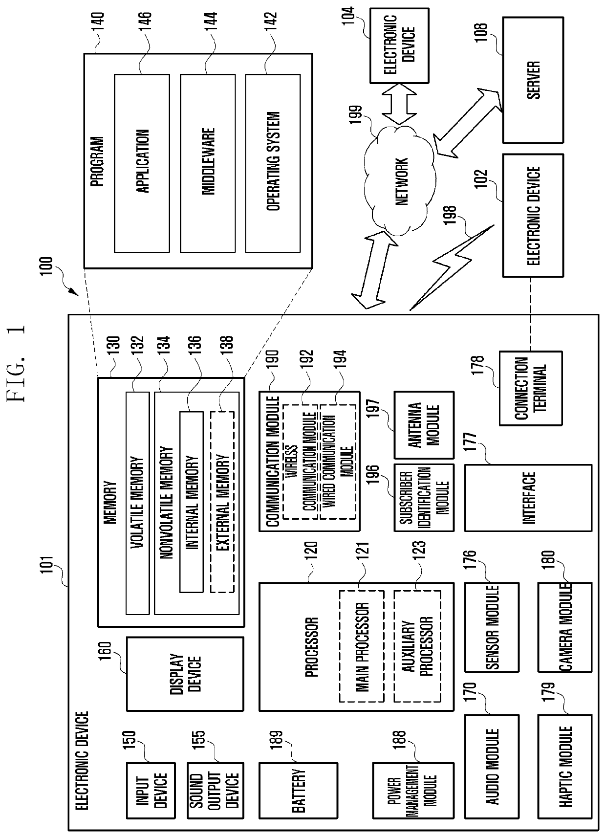
[0028]FIG. 1 illustrates an electronic device in a network environment according to an embodiment of the disclosure.

[0029]Referring to FIG. 1, an electronic device 101 in a network environment 100 may communicate with an electronic device 102 via a first network 198 (e.g., a short-range wireless communication network), or an electronic device 104 or a server 108 via a second network 199 (e.g., a long-range wireless communication network). The electronic device 101 may communicate with the electronic device 104 via the server 108. The electronic device 101 includes a processor 120,...


PUM


Abstract

According to various embodiments, an electronic device may comprise: a housing; an antenna structure disposed in an inner space of the housing, the antenna structure including a substrate having a first surface and a second surface oriented toward a direction opposite to the first surface, and at least one first antenna element disposed in a space between the first surface and the second surface and having a beam pattern formed toward a conductive part; an electric wave absorbing member disposed between the conductive part and the at least one first antenna element so as to be disposed in a path in which the beam pattern is formed; and a first wireless communication circuit disposed in the inner space of the housing and configured to transmit or receive a wireless signal of a first frequency band through the at least one first antenna element.

Description

CROSS-REFERENCE TO RELATED APPLICATIONS[0001]This application is a Bypass Continuation of International Application No. PCT / KR2020 / 006697, filed May 22, 2020, which claims priority to Korean Patent Application No. 10-2019-0070126, filed Jun. 13, 2019, the disclosures of which are herein incorporated by reference in their entirety.BACKGROUND1. Field[0002]Various embodiments of the disclosure relate to an antenna and an electronic device including the same.2. Description of Related Art[0003]Electronic devices (for example, electronics device for communication) are widely used in daily life in line with development of wireless communication technologies, and use of contents resulting therefrom is increasing exponentially. Network capacities are gradually reaching limits as a result of such an abrupt increase in content use, and in order to satisfy wireless data traffic demands that have been increasing since commercialization of 4G (4th generation) communication systems, there has been...

Claims


Application Information

Patent Timeline
Patent Type & Authority Applications(United States)
IPC IPC(8): H01Q17/00H01Q1/24
CPCH01Q17/004H01Q1/243H04M1/02H04B1/40H01Q17/001H01Q17/00H04M1/0249H04M1/0277H01Q1/38
Inventor PARK, SUNGCHUL
Owner SAMSUNG ELECTRONICS CO LTD
Learn More