
Resistive memory device and method for reading data in the resistive memory device

a resistive memory and data technology, applied in the direction of information storage, static storage, digital storage, etc., can solve the problem of inability to read data in the resistive memory device, and the size of the memory cell array may have inevitably increased, so as to improve the reliability of sensing

Pending Publication Date: 2022-03-10
SAMSUNG ELECTRONICS CO LTD
View PDF7 Cites 0 Cited by
  • Summary
  • Abstract
  • Description
  • Claims
  • Application Information

AI Technical Summary

Benefits of technology

This patent is about a new type of memory device called resistive memory, which can be made smaller and more reliable by improving the way it senses data. The patent also explains a method for reading data from this improved memory device. The technical effect of this innovation is to make memory devices faster, more efficient, and more reliable as they get smaller.

Problems solved by technology

The volatile memory may lose information stored therein each time power is removed, whereas the nonvolatile memory may retain data stored therein even when power is removed from the memory.
However, there may be many restrictions on the reading conditions of the memory cell, or the size of a memory cell array may have inevitably increased according to the characteristics of the sensing operation.

Method used


Image

  • Resistive memory device and method for reading data in the resistive memory device
  • Resistive memory device and method for reading data in the resistive memory device
  • Resistive memory device and method for reading data in the resistive memory device

Examples


Embodiment Construction

[0025]Hereinafter, embodiments of the disclosure will be described with reference to the accompanying drawings.

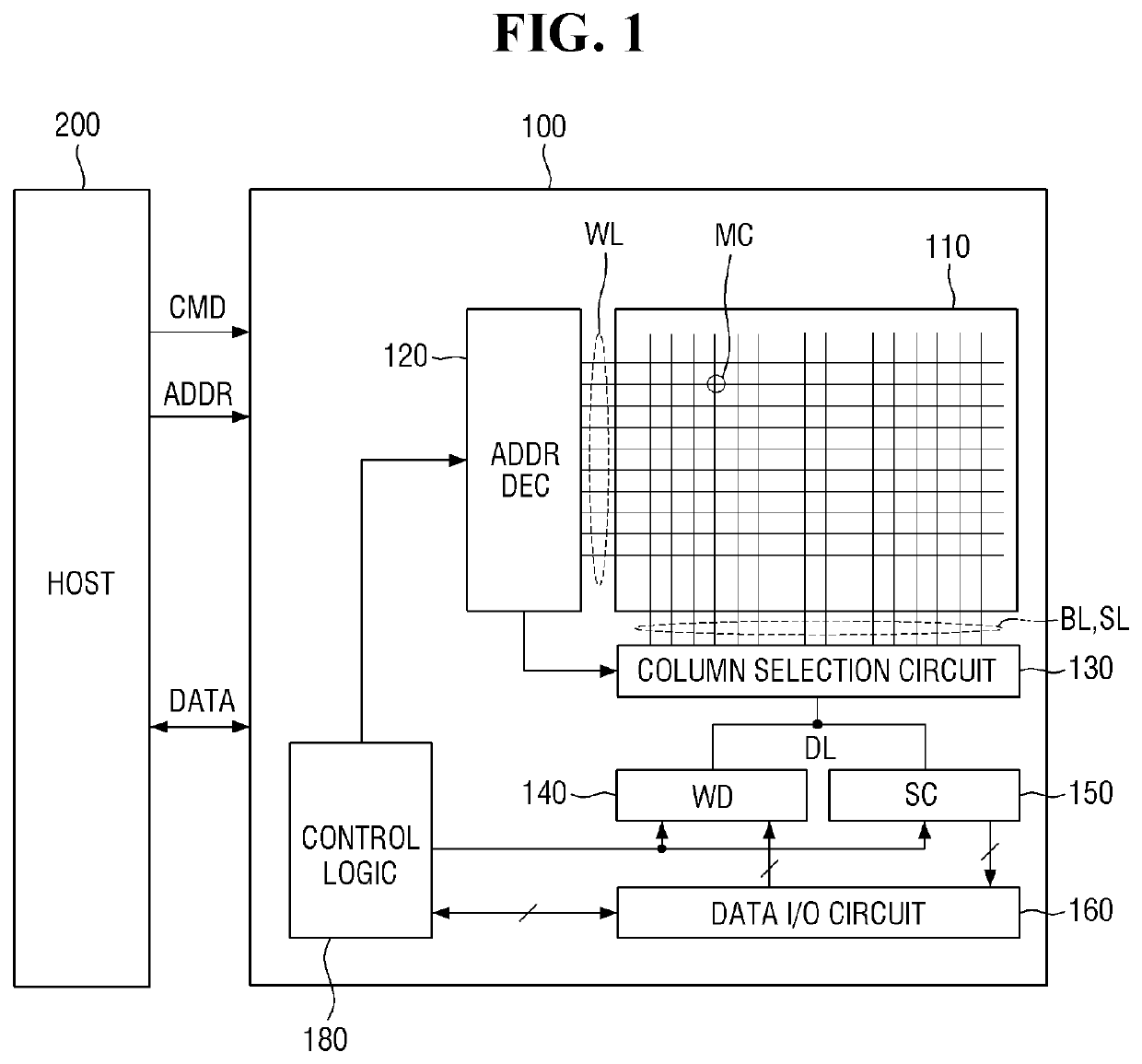
[0026]FIG. 1 is a diagram for describing a nonvolatile memory device according to embodiments.

[0027]Referring to FIG. 1, a nonvolatile memory device 100 may read or write data in response to a request from a host 200.

[0028]The nonvolatile memory device 100 may receive a command CMD and an address ADDR from the host 200. The command CMD may include a read command, a write command, and the like. When the host 200 transmits the read command to the nonvolatile memory device 100, the nonvolatile memory device 100 may provide data read from a memory cell array 110 to the host 200.

[0029]When the host 200 transmits the write command and the data DATA to be written to the nonvolatile memory device 100, the nonvolatile memory device 100 may write the data DATA provided from the host 200 to the memory cell array 110.

[0030]The nonvolatile memory device 100 may include the memory cell a...


PUM


Abstract

A resistive memory device includes a resistive memory cell, a source line connected to one end of the resistive memory cell, a bit line connected to another end of the resistive memory cell, and a sensing circuit connected to the source line and the bit line. The sensing circuit is configured to generate a pull-up signal that is pulled up from a first voltage level to a second voltage level, based on a read current flowing through the resistive memory cell, generate a pull-down signal that is pulled down from a third voltage level to a fourth voltage level, based on the read current, and determine data that is stored in the resistive memory cell, based on a difference between the generated pull-up signal and the generated pull-down signal.

Description

CROSS-REFERENCE TO RELATED APPLICATION[0001]This application is based on and claims priority under 35 U.S.C. § 119 to Korean Patent Application No. 10-2020-0115164 filed on Sep. 9, 2020, in the Korean Intellectual Property Office, the disclosure of which is incorporated by reference herein in its entirety.BACKGROUND1. Field[0002]The disclosure relates to a resistive memory device and a method for reading data in the resistive memory device.2. Description of Related Art[0003]A random access memory (RAM) may include a volatile memory and a nonvolatile memory. The volatile memory may lose information stored therein each time power is removed, whereas the nonvolatile memory may retain data stored therein even when power is removed from the memory.[0004]The nonvolatile memory may include a resistive memory that stores data according to a resistance change of a memory cell. A spin torque transfer-magnetic random access memory (STT-MRAM), which is a type of the nonvolatile memory, may read...

Claims


Application Information

Patent Timeline
Patent Type & Authority Applications(United States)
IPC IPC(8): G11C13/00G11C11/16
CPCG11C13/004G11C13/0026G11C13/0038G11C2213/79G11C11/1655G11C2013/0045G11C11/1673G11C13/0009G11C11/1659G11C7/04
Inventor KIM, CHAN KYUNG
Owner SAMSUNG ELECTRONICS CO LTD
Learn More