Solid-state imaging device and method for manufacturing the same

a technology of solid-state imaging and imaging device, which is applied in the direction of color television, television system, radioation control device, etc., can solve the physical limitations of higher integration of two-dimensional structure by these methods, and achieve the effect of reducing bonding defects

Pending Publication Date: 2021-06-03
SONY SEMICON SOLUTIONS CORP
View PDF2 Cites 0 Cited by
  • Summary
  • Abstract
  • Description
  • Claims
  • Application Information

AI Technical Summary

Benefits of technology

[0012]According to one aspect of the present technology, bonding defects can be reduced when two substrates are bonded to each other.
[0013]Note that the effects of the present technology are not limited to the effect described herein, and may include any of the effects described in the present disclosure.

Problems solved by technology

However, there are physical limitations to higher integration of two-dimensional structures by these methods.

Method used


Image

  • Solid-state imaging device and method for manufacturing the same
  • Solid-state imaging device and method for manufacturing the same
  • Solid-state imaging device and method for manufacturing the same

Examples


first embodiment

2. First Embodiment

[0055](Structure of the Bonding Portion)

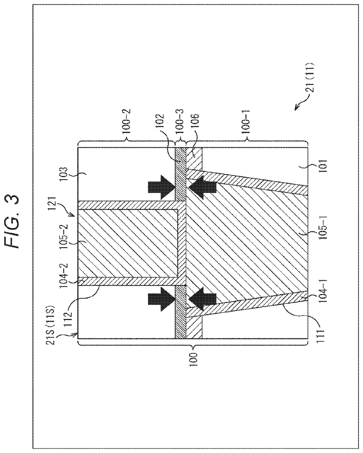
[0056]FIG. 3 is a cross-sectional view of relevant parts, showing the structure of a solid-state imaging device 1 according to the first embodiment. In the description below, the configuration of the solid-state imaging device 1 according to the first embodiment is specifically described, with reference to the cross-sectional view of the relevant parts.

[0057]Note that, of the first substrate 11 and the second substrate 21 bonded in the solid-state imaging device 1, the second substrate 21 will be described as a typical example with reference to FIG. 3, but the first substrate 11 may have a similar structure (the structure of the first embodiment). Further, the surface on the upper side in the drawing is a bonding surface 21S of the second substrate 21 or a bonding surface 11S of the first substrate 11.

[0058]In FIG. 3, a laminated film 100 in which a first layer 100-1 and a second layer 100-2 are stacked is formed in the seco...

second embodiment

3. Second Embodiment

[0108](Structure of the Bonding Portion)

[0109]FIG. 9 is a cross-sectional view of relevant parts, showing the structure of a solid-state imaging device according to a second embodiment. In the description below, the configuration of a solid-state imaging device 1 according to the second embodiment is specifically described, with reference to the cross-sectional view of the relevant parts.

[0110]Note that, of a first substrate 11 and a second substrate 21 bonded in the solid-state imaging device 1, the second substrate 21 will be described as a typical example with reference to FIG. 9, but the first substrate 11 may have a similar structure (the structure of the second embodiment).

[0111]In FIG. 9, a laminated film 200 in which a first layer 200-1 and a second layer 200-2 are stacked is formed in the second substrate 21.

[0112]In the first layer 200-1, a via 211 is formed in an interlayer insulating film 201 made of silicon oxide (SiO2) or the like, and a metallic fi...


PUM

PropertyMeasurementUnit
speedaaaaaaaaaa
diameteraaaaaaaaaa
packaging densityaaaaaaaaaa

Abstract

The present technology relates to a solid-state imaging device capable of reducing bonding defects when two substrates are bonded to each other, and a method for manufacturing the solid-state imaging device. The present technology provides a solid-state imaging device that includes: a first substrate including a first electrode formed with a metal; and a second substrate that is a substrate bonded to the first substrate, the second substrate including a second electrode formed with a metal, the second electrode being bonded to the first electrode. In at least one of the first substrate or the second substrate, a diffusion preventing layer of the metal is formed for a layer formed with the metal filling a hole portion, the metal forming the electrodes. The present technology can be applied to solid-state imaging devices, such as CMOS image sensors, for example.

Description

TECHNICAL FIELD[0001]The present technology relates to a solid-state imaging device and a method for manufacturing the solid-state imaging device, and more particularly, to a solid-state imaging device capable of reducing bonding defects when two substrates are bonded to each other, and a method for manufacturing the solid-state imaging device.BACKGROUND ART[0002]Higher integration of semiconductor devices of two-dimensional structures has been realized through introduction of fine processing and enhancement of packaging density. However, there are physical limitations to higher integration of two-dimensional structures by these methods. Therefore, to further reduce the sizes of semiconductor devices and increase the pixel density, semiconductor devices having three-dimensional structures are being developed.[0003]For example, Patent Document 1 discloses a stack semiconductor device in which two semiconductor devices are stacked. Patent Document 1 also discloses a technique of provi...

Claims


Application Information

Patent Timeline
Patent Type & Authority Applications(United States)
IPC IPC(8): H01L27/146H04N5/374
CPCH01L27/14621H01L27/14609H01L27/14683H04N5/374H01L21/768H01L27/1469H01L27/14636H01L27/14634H04N25/76
Inventor FUKASAWA, MASANAGA
Owner SONY SEMICON SOLUTIONS CORP
Why Eureka
Try Eureka