Electronic module

Active Publication Date: 2020-07-30
SHINDENGEN ELECTRIC MFG CO LTD
View PDF0 Cites 0 Cited by
  • Summary
  • Abstract
  • Description
  • Claims
  • Application Information

AI Technical Summary

Benefits of technology

The present invention improves the connection between two electrical components by adjusting the distance between the rear surfaces of the two parts. This allows for the second connector to be securely placed and prevents defective connections, improving reliability.

Problems solved by technology

In such an electronic module, since a control electrode (gate electrode) of an electronic element is smaller than the other input / output electrodes (source electrode and drain electrode), it is difficult to connect a control electrode and a connector, and it is necessary to stably connect one end of a lead terminal such that the connector does not fall sideways.
If a defect occurs in connection of the connector, the controllability of an electronic element is deteriorated, and the reliability of an electronic module is deteriorated.

Method used


Image

  • Electronic module
  • Electronic module
  • Electronic module

Examples


first embodiment

>

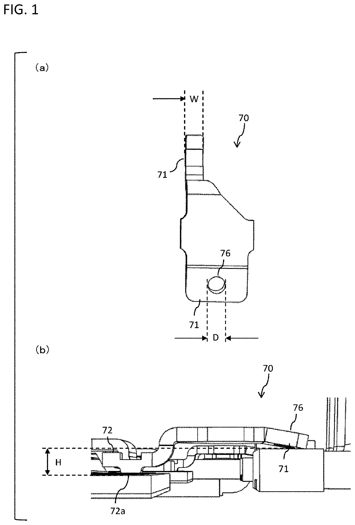
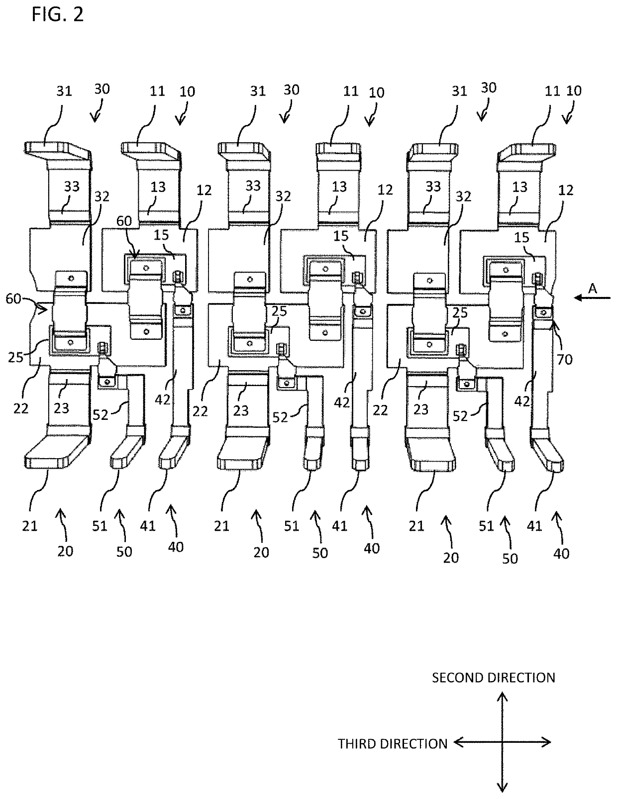
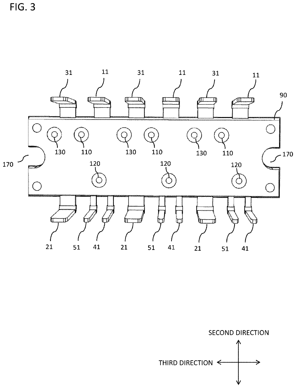
[0057]As illustrated in FIG. 2, an electronic module according to the present embodiment may have a sealing part 90 (refer to FIG. 3), rear surface-exposed conductors 10, 20 and 30, which have rear surface exposed-side terminal parts 11, 21 and 31 protruding outwardly from a side surface of the sealing part 90 and rear surface-exposed parts 12, 22 and 32 (refer to FIG. 8) whose rear surface is exposed, rear surface-unexposed conductors 40 and 50, which have rear surface unexposed-side terminal parts 41 and 51 protruding outwardly from a side surface of the sealing part 90 and whose rear surface is not exposed, a plurality of electronic elements 15 and 25, which is provided in the sealing part 90 and provided on a front surface of the rear surface-exposed conductors 10, 20, and 30 via a conductive adhesive 190 (refer to FIG. 11) such as solder, and connectors 60 and 70, which have a first connector 60 and a second connector 70. The connectors 60 and 70 have a first connector 60 and ...

second embodiment

[0112]Next, a second embodiment of the present invention will be described.

[0113]As indicated in FIG. 12, grooves 150 may be provided on the front surfaces of the rear surface-exposed parts 12, 22, and 32 of the rear surface-exposed conductors 10, 20, and 30. As indicated in FIG. 12, the groove 150 may be provided in each of the rear surface-exposed conductors 10, 20, and 30 or may be provided only in a part of the rear surface-exposed conductors 10, 20, and 30. As indicated in FIG. 13, in the longitudinal direction of the sealing part 90 in the in-plane direction, the center portion of the press holes or press impressions 110, 120, and 130 may be provided on the side opposite to the connectors 60 and 70 or the electronic elements 15 and 25 with respect to the groove 150. The groove 150 of the present embodiment does not penetrate through the rear surface-exposed parts 12, 22, and 32, and the recesses formed in the rear surface-exposed parts 12, 22, and 32 are the grooves 150. Howev...

third embodiment

[0125]Next, a third embodiment of the present invention will be described.

[0126]In the present embodiment, as illustrated in FIG. 14, the rear surface-exposed conductors 10, 20, and 30 are provided between the rear surface-exposed parts 12, 22, and 32 and the rear surface exposed-side terminal parts 11, 21 and 31, and the connected parts 16, 26 and 36 whose rear surface is not exposed are provided. More specifically, the connected parts 16, 26 and 36 whose rear surface is not exposed are provided between the internal bent parts 13, 23, and 33 and the rear surface-exposed parts 12, 22, and 32. The thickness of the connected parts 16, 26 and 36 is thinner than the thickness of the rear surface-exposed parts 12, 22, and 32 and the thickness of the rear surface exposed-side terminal parts 11, 21 and 31. For example, the thickness of the rear surface-exposed parts 12, 22, and 32 and the thickness of the rear surface exposed-side terminal parts 11, 21 and 31 are substantially the same, an...


PUM


Abstract

An electronic module comprises a sealing part 90, a rear surface-exposed conductor 10, 20, 30, a rear surface-unexposed conductor 40, 50 and a second connector 70 for electrically connecting an electronic element 15, 25 to the rear surface-unexposed conductor 40, 50. The rear surface-unexposed conductor 40, 50 is positioned on a front surface side compared with the rear surface-exposed part 12, 22, 32. The second connection tip part 72 is positioned on a rear surface side compared with the second connection base part 71. A distance H in a thickness direction between a rear surface side end part of the second connection base part 71 and a rear surface side end part of the second connection tip part 72 is larger than a width W of the second connection tip part 72 of the second connector 70.

Description

TECHNICAL FIELD[0001]The present invention relates to an electronic module having a rear surface-exposed part whose rear surface is exposed from a sealing part.BACKGROUND ART[0002]In conventional electronic modules, control electrodes (gate electrodes) and lead terminals (lead frames) of high-side and low-side electronic elements (MOSFETs) are soldered with connectors (gate clips) (for example, refer to JP 2002-100716 A and JP 2009-238859 A).[0003]In such an electronic module, since a control electrode (gate electrode) of an electronic element is smaller than the other input / output electrodes (source electrode and drain electrode), it is difficult to connect a control electrode and a connector, and it is necessary to stably connect one end of a lead terminal such that the connector does not fall sideways.[0004]If a defect occurs in connection of the connector, the controllability of an electronic element is deteriorated, and the reliability of an electronic module is deteriorated.SU...

Claims


Application Information

Patent Timeline
IPC IPC(8): H01L23/495H01L23/31H01L23/00
CPCH01L23/49524H01L23/49562H01L2224/3701H01L23/49551H01L24/40H01L2924/183H01L24/37H01L23/49575H01L23/31H01L2224/4103H01L2924/181H01L2224/40245H01L2224/37013H01L2224/37011H01L2224/84801H01L24/41H01L24/45H01L24/84H01L2224/37147H01L2224/45124H01L2224/4099H01L23/49548H01L24/29H01L2224/0603H01L2224/26175H01L2924/1815H01L2924/18301H01L2224/29101H01L2924/13091H01L2224/84345H01L2924/00014H01L2924/00012H01L2924/014H01L2924/00H01L2224/73221
Inventor KAMIYAMA, YOSHIHIRO
Owner SHINDENGEN ELECTRIC MFG CO LTD
Why Eureka
Try Eureka