Systems, devices, and methods to interact with quantum information stored in spins

a technology of quantum information and spins, applied in the field of quantum computing and quantum information, can solve problems such as unfulfilled realization of proposed techniques

Active Publication Date: 2018-11-15
PHOTONIC INC
View PDF0 Cites 20 Cited by
  • Summary
  • Abstract
  • Description
  • Claims
  • Application Information

AI Technical Summary

Benefits of technology

[0008]Another method of operation for a quantum information processor including a non-gaseous chalcogen donor atom disposed in a semiconductor substrate. The non-gaseous chalcogen donor atom is characterized as having one or more different quantum states representing information. In one as...

Problems solved by technology

The proposed technique...

Method used


Image

  • Systems, devices, and methods to interact with quantum information stored in spins
  • Systems, devices, and methods to interact with quantum information stored in spins
  • Systems, devices, and methods to interact with quantum information stored in spins

Examples


example 1

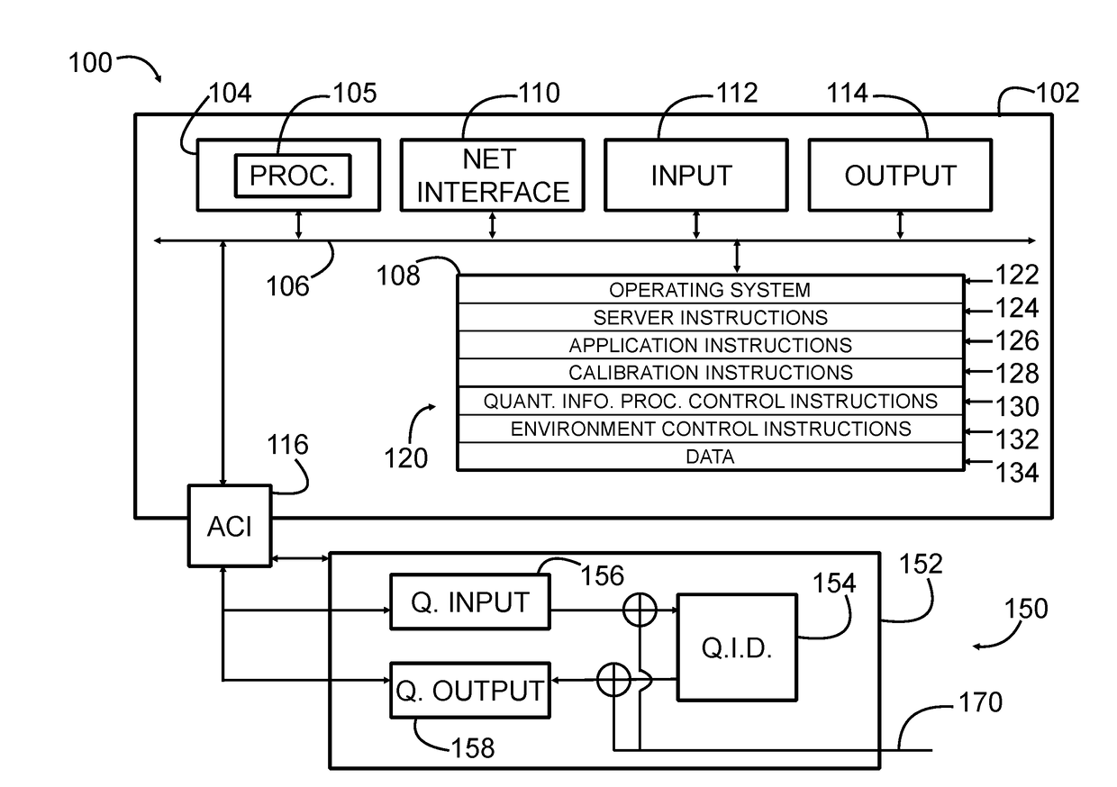
[0168]A quantum information processing device comprising: a semiconductor substrate; one or more deep impurities disposed within the semiconductor substrate, wherein each of the deep impurities is characterized by a plurality of quantum states corresponding to different electron or nuclear spin states of the deep impurity and representing qubit information; one or more optical structures integrated with or coupled to the semiconductor substrate, each optical structure having a characteristic mode frequency and an optical state representing optical structure information; and a first deep impurity optically coupled to a first optical structure, the first deep impurity having a first transition frequency between a first pair of the plurality of quantum states, the first transition frequency matching a first characteristic mode frequency of the first optical structure, wherein the first optical structure optically couples the qubit information and the optical structure information.

example 2

[0169]The device of example 1, wherein the characteristic mode frequency of the optical structure is a resonant mode frequency.

example 3

[0170]The device of example 1, wherein the characteristic mode frequency of the first optical structure is a propagating mode frequency.


PUM


Abstract

A quantum information processing device including a semiconductor substrate. An optical resonator is coupled to the substrate. The optical resonator supports a first photonic mode with a first resonator frequency. The quantum information processing device includes a non-gaseous chalcogen donor atom disposed within the semiconductor substrate and optically coupled to the optical resonator. The donor atom has a transition frequency in resonance with the resonator frequency. Also disclosed herein are systems, devices, articles and methods with practical application in quantum information processing including or associated with one or more deep impurities in a silicon substrate optically coupled to an optical structure.

Description

CROSS REFERENCE TO RELATED APPLICATION[0001]This application is a non-provisional of, and claims priority to, U.S. Patent Application No. 62 / 260,391, filed on Nov. 27, 2015, entitled “SYSTEMS, DEVICES, AND METHODS FOR INTERACTING WITH QUANTUM INFORMATION STORED IN SPINS”, which is incorporated by reference herein in its entirety.BACKGROUNDTechnical Field[0002]This disclosure generally relates to the fields of quantum computing and quantum information.Description of the Related Art[0003]Quantum devices are manufactures or structures in which quantum mechanical effects are noticeable and / or dominate. Quantum devices (such as superconducting circuits and spintronic circuits) include circuits in which current transport is dominated by quantum mechanisms. Superconducting circuits use quantum physics phenomena such as tunneling and flux quantization. Spintronic circuits use the physical property of spin (e.g. electron spin) as a resource to receive, process, store, send, or output informa...

Claims


Application Information

Patent Timeline
IPC IPC(8): G06N99/00H01L29/06G02B6/12H01L29/167H01L29/66H01L29/82H01L27/20
CPCG06N99/002H01L29/0684G02B6/12H01L29/167H01L29/66984H01L29/82H01L27/20H01L29/161H01L29/1608G02B2006/12061B82Y10/00H01L29/36H01L29/66977H01L29/127H01L29/0665H01L29/0692G06N10/00G02B6/29341G02B6/1225G02B6/12007G02B6/26H10N39/00
Inventor SIMMONS, STEPHANIETHEWALT, MICHAEL L. W.
Owner PHOTONIC INC
Why Eureka
Try Eureka