Semiconductor device driving device
a driving device and semiconductor technology, applied in the direction of electronic switching, pulse technique, power conversion system, etc., can solve the problems of large time delay in overcurrent detection and difficulty in revising the device structure of igbt b>2
- Summary
- Abstract
- Description
- Claims
- Application Information
AI Technical Summary
Benefits of technology
Problems solved by technology
Method used
Image
Examples
embodiment 1
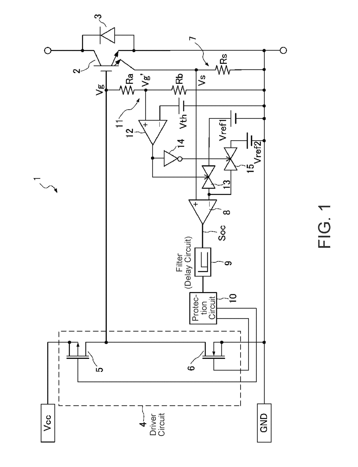
[0036]FIG. 1 schematically illustrates a configuration of the primary components of a semiconductor device driving device of the present invention. Note that the same reference characters are used for components which are the same as in the conventional semiconductor device driving device 1 illustrated in FIG. 9, and descriptions of such components will be omitted here.
[0037]One characterizing feature of a semiconductor device driving device 1 according to the present embodiment is the inclusion of a gate voltage detection circuit 11 for detecting the gate voltage of an IGBT 2 in addition to the basic configuration included in the driving device 1 illustrated in FIG. 9. This gate voltage detection circuit 11 includes a voltage-dividing circuit which is constituted by series-connected voltage-dividing resistors Ra and Rb and divides and detects a gate voltage Vg of the IGBT 2. A comparator 12 compares a gate detection voltage Vg′, which is detected as the gate voltage detection circ...
embodiment 2
[0058]Next, a semiconductor device driving device 1 of the present disclosure will be described with reference to FIG. 7.
[0059]The driving device 1 according to Embodiment 2 includes, in addition to the basic configuration of the driving device 1 illustrated in FIG. 1, a second low-pass filter circuit 16 connected in parallel to the low-pass filter circuit 9. When the gate voltage Vg is higher than the gate reference voltage VTH, this second low-pass filter circuit 16 is activated upon receiving the overcurrent detection signal Soc output by the comparator 8 via an AND gate circuit 17 in which the gate is opened upon receipt of the output of the comparator 12. When the gate voltage Vg is lower than the gate reference voltage VTH, the low-pass filter circuit 9 is activated upon receiving the overcurrent detection signal Soc output by the comparator 8 via an AND gate circuit 18 in which the gate is opened upon receipt of the output of the inverting circuit 14. In other words, the AND...
PUM
 Abstract
Description
Claims
Application Information
 - Generate Ideas
- Intellectual Property
- Life Sciences
- Materials
- Tech Scout
- Unparalleled Data Quality
- Higher Quality Content
- 60% Fewer Hallucinations
Browse by: Latest US Patents, China's latest patents, Technical Efficacy Thesaurus, Application Domain, Technology Topic, Popular Technical Reports.
© 2025 PatSnap. All rights reserved.Legal|Privacy policy|Modern Slavery Act Transparency Statement|Sitemap|About US| Contact US: help@patsnap.com


