Semiconductor device

a technology of semiconductors and devices, applied in the field of semiconductor devices, can solve problems such as the increase of the probability of errors

Active Publication Date: 2018-09-20
SK HYNIX INC
View PDF4 Cites 3 Cited by
  • Summary
  • Abstract
  • Description
  • Claims
  • Application Information

AI Technical Summary

Benefits of technology

[0005]According to an embodiment, a semiconductor device may be provided. The semiconductor device may include an input and output (I / O) control circuit and an I / O circuit. The I / O control circuit may be configured to delay a write signal by a delay time to generate a write enablement signal. The I / O circuit may be configured to output transfer data generated from input data as internal data based on the write enablement signal. The I / O circuit may be configured to output a parity including error information on the input data as an internal parity based on the write enablement signal. The delay time may be controlled according to whether an error correction operation is performed.

Problems solved by technology

If data transmission speeds of the semiconductor devices become faster, probability of error occurrence may increase while the data is transmitted within the semiconductor devices.

Method used


Image

  • Semiconductor device
  • Semiconductor device
  • Semiconductor device

Examples


Embodiment Construction

[0020]Various embodiments of the present disclosure will be described hereinafter with reference to the accompanying drawings. However, the embodiments described herein are for illustrative purposes only and are not intended to limit the scope of the present disclosure.

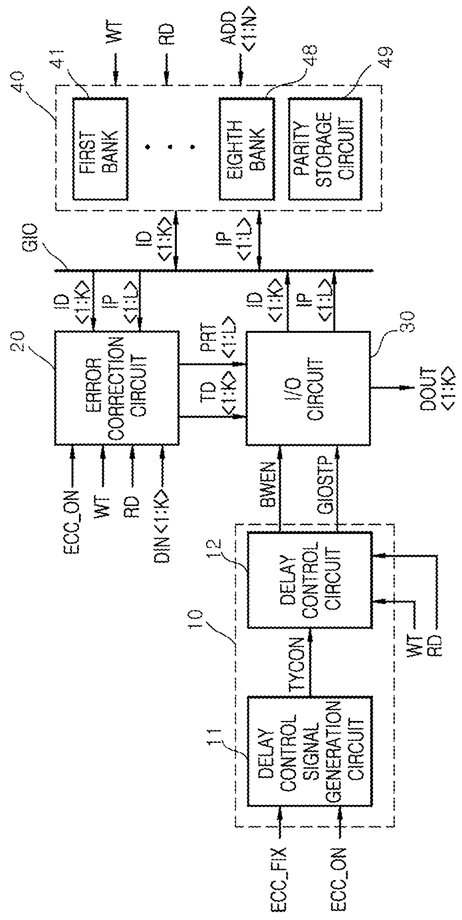
[0021]Various embodiments may be directed to semiconductor devices executing an error correction operation.

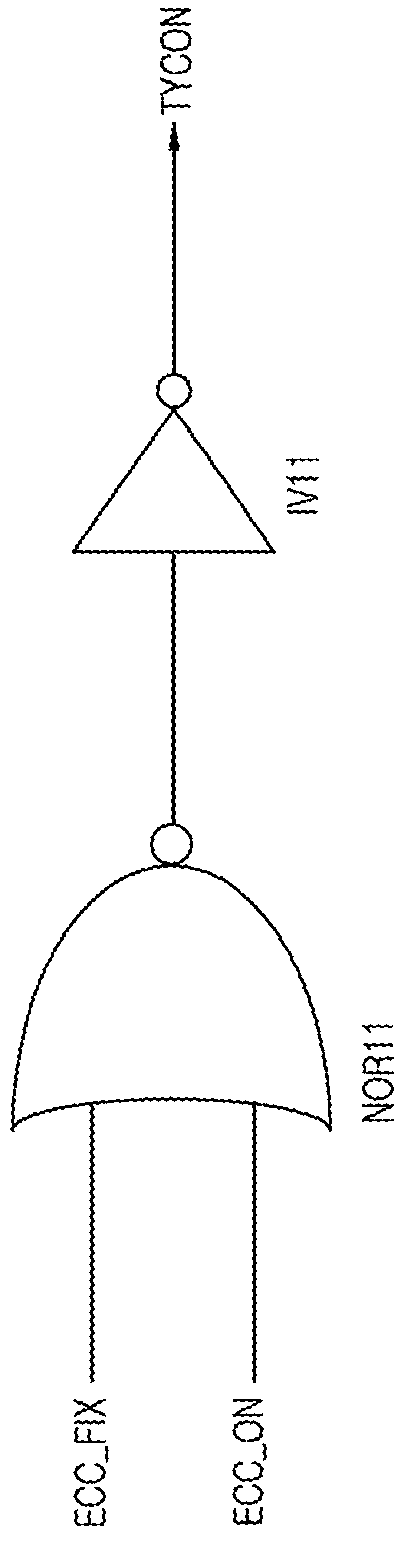
[0022]For reference, an embodiment including additional components may be provided. Furthermore, an logic high or logic low configuration indicating an active state of a signal or circuit may be changed depending on embodiments. Furthermore, the configuration of a logic gate or logic gates required for implementing the same function or operation may be modified. That is, the logic gate configuration of one type of operation and another logic gate configuration for the same type of operation may be replaced with each other, depending on a specific situation. If necessary, various logic gates may be applied to impl...


PUM


Abstract

A semiconductor device may be provided. The semiconductor device may include an input and output (I/O) circuit configured to output transfer data generated from input data as internal data based on a write enablement signal and configured to output error information on the input data based on the write enablement signal. The generation of the write enablement signal may be based on a write signal which may be delayed by a delay time according to whether an error correction operation is performed.

Description

CROSS-REFERENCE TO RELATED APPLICATIONS[0001]The present application claims priority under 35 U.S.C 119(a) to Korean Application No. 10-2017-0034875, filed on Mar. 20, 2017, which is incorporated herein by reference in its entirety.BACKGROUND1. Technical Field[0002]Embodiments of the present disclosure may generally relate to a semiconductor device configured for executing an error correction operation.2. Related Art[0003]Recently, a DDR2 scheme or a DDR3 scheme receiving and outputting four-bit data or eight-bit data during each clock cycle time has been used to improve operation speeds of the semiconductor devices. If data transmission speeds of the semiconductor devices become faster, probability of error occurrence may increase while the data is transmitted within the semiconductor devices. Accordingly, novel design schemes may be required to guarantee reliable transmission of the data.[0004]Whenever the data is transmitted within the semiconductor devices, error codes which are...

Claims


Application Information

Patent Timeline
Patent Type & Authority Applications(United States)
IPC IPC(8): H03M13/11H03K5/15G06F11/10H03M13/00
CPCH03M13/1111H03K5/15G06F11/10H03M13/611G06F11/1012G11C7/1057G11C7/1084G11C29/04G11C2029/0411G06F11/1048G06F11/1008G11C29/42
Inventor LEE, JAE INKIM, YONG MI
Owner SK HYNIX INC
Why Eureka
Try Eureka