Wafer de-bonding device

a technology of debonding device and wafer, which is applied in the field of microelectronics technology, can solve the problems of easy breakage or bendage, difficult to process such ultra-thin wafer directly, and take a long time for solvent to reach, etc., and achieves the effect of simple and convenient operation and stable gas j

Inactive Publication Date: 2018-04-19
MICRO MATERIALS INC
View PDF13 Cites 8 Cited by
  • Summary
  • Abstract
  • Description
  • Claims
  • Application Information

AI Technical Summary

Benefits of technology

[0014]In a preferred embodiment, the gas outlet may be provided on the upper surface of the bit of the tool. With such a configuration, the gas jet may blow through the gas outlet while the tool bit cuts a notch, thereby achieving simple and convenient operations.
[0015]There may be two gas outlets provided in the upper surface of the tool bit, and a tapered slot provided in a side surface of the tool. Using two gas outlets may make the gas jet more stable, and the tapered slot may accommodate a gas tube connected to the gas inlet as well the image acquisition device and cables connected to the image acquisition device.

Problems solved by technology

When a Silicon wafer is thinned to a thickness of 100 microns or less, however, it may easily break or bend due to stress applied thereon during processing.
As a result, it is almost impossible to process such an ultra-thin wafer directly.
With the first method, the solvent dissolves the bonding adhesive slowly from the edge of the junction where the device wafer and carrier wafer are bonded together, and it will take a long time for the solvent to reach the center of the device wafer, resulting in a very low efficiency.
In addition, it needs a special plate to secure the device wafer so as to prevent the device wafer from mixing with the carrier wafer while separating them, which causes a complex procedure and a high cost.
As to the second method, it needs a special equipment to carry out the thermal shearing process, which also causes a high cost, and the thermal shearing process is easy to damage the device wafer and thus has a low yield.

Method used


Image

  • Wafer de-bonding device
  • Wafer de-bonding device
  • Wafer de-bonding device

Examples


Embodiment Construction

[0021]The present invention will be described in detail below with reference to the accompanying drawings and specific embodiments.

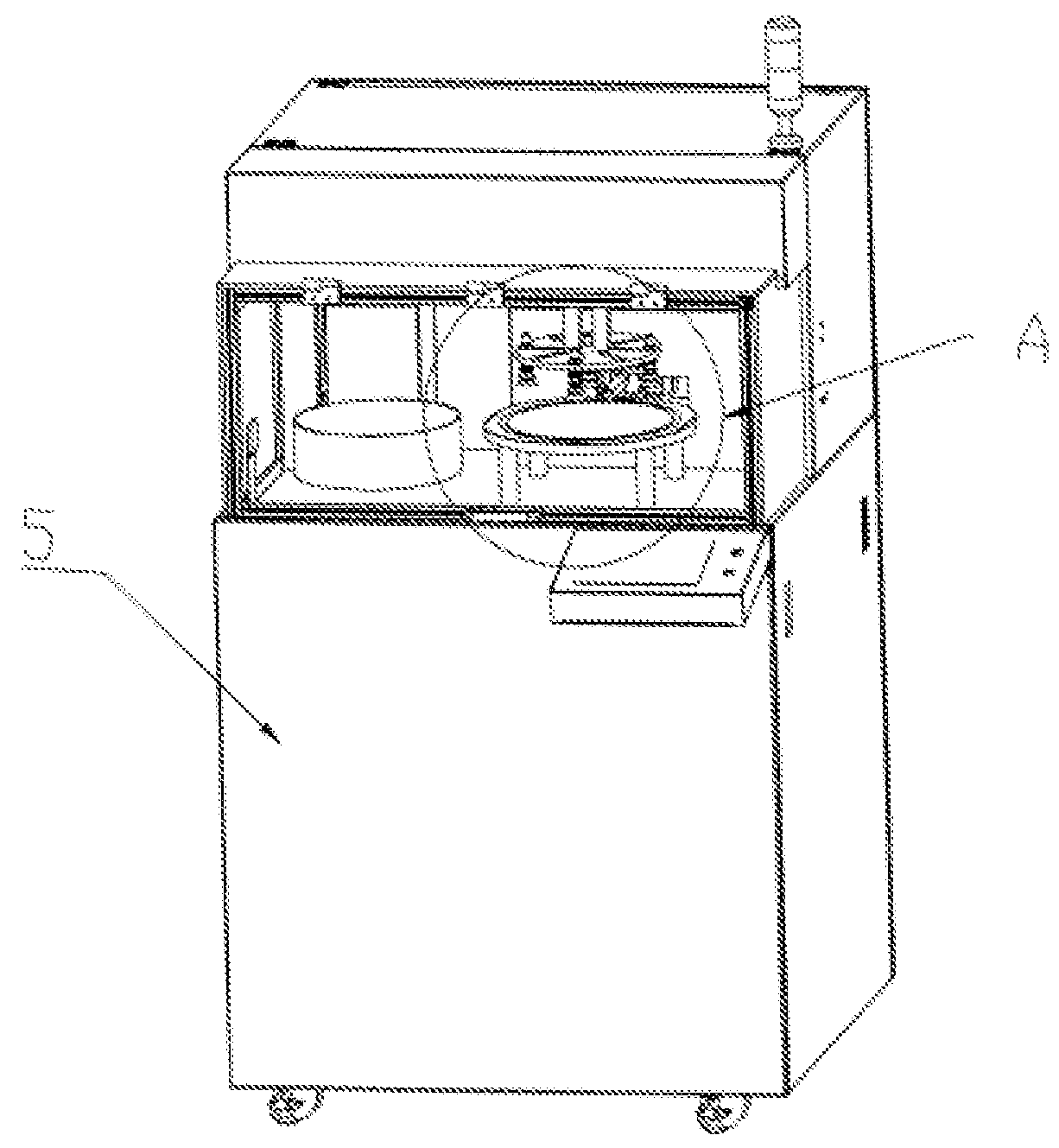
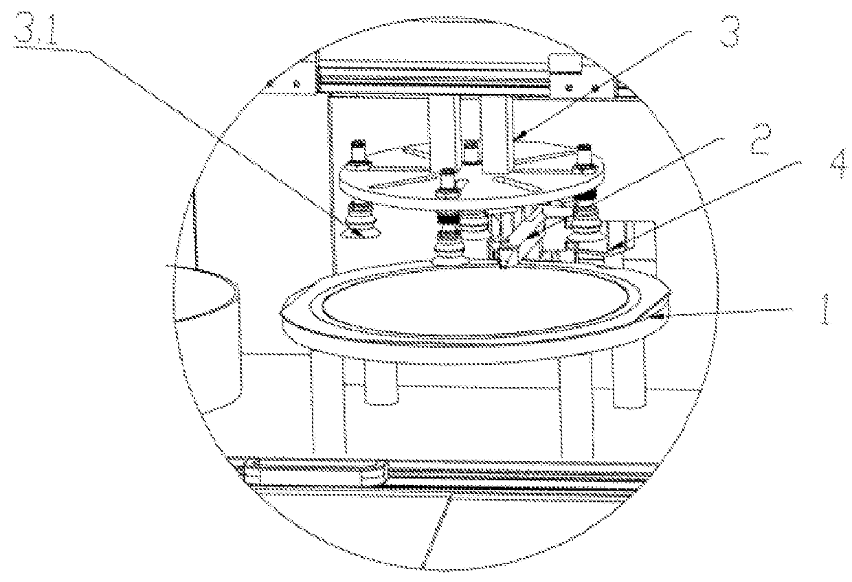
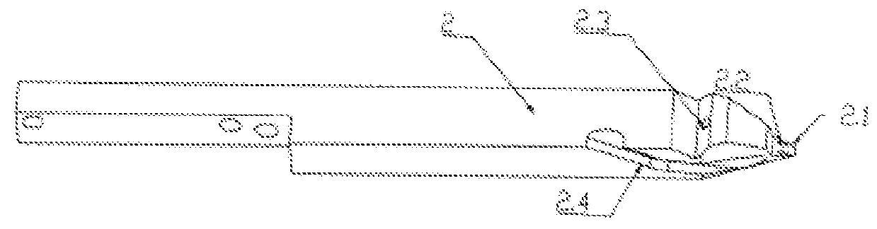
[0022]As shown in FIGS. 1-4, the present invention provides a wafer de-bonding device including a stage 1 for holding bonded wafers, and a tool 2 with a gas outlet 2.2 disposed in proximity to the stage and mounted to an adjustment device which controls the tool 2 to move towards or away from the stage 1. The adjustment device may include a displacement mechanism such as an electric cylinder or a gas cylinder and a step motor to finely adjust position of the tool 2, which belongs to prior arts and will not be described in detail here. The tool 2 is provided with a bit 2.1, which may be used to cut a notch at a junction of the bonded device wafer and carrier wafer. The gas outlet 2.2 may be disposed in an upper surface of the tool bit 2.1. In other embodiments, of course, the gas outlet 2.2 may also be disposed in a lower surface of the tool bit 2.1 to di...


PUM

PropertyMeasurementUnit
thicknessaaaaaaaaaa
coloraaaaaaaaaa
temperatureaaaaaaaaaa

Abstract

A wafer de-bonding device comprises a stage (1) for holding a device wafer and a carrier wafer bonded together, and a tool (2) with a gas outlet (2.2) disposed in proximity to the stage (1) through an adjustment device for control the tool (2) to move towards or away from the stage (1), the tool (2) being provided with a bit (2.1) to cut a notch into a film or an adhesive layer at a junction of the bonded wafers, the gas outlet (2.2) being provided on the tool bit (2.1), the tool (2) being further provided with a gas inlet (2.3) in communication with the gas outlet (2.2), the gas inlet (2.3) being connected to a gas jet generator so as to direct a gas jet towards the junction of the bonded wafers on the stage (2). The wafer de-bonding device has a high degree of automation and simple operations.

Description

FIELD OF THE INVENTION[0001]The present invention relates to the field of microelectronics technology, and more particularly, to a wafer de-bonding device.BACKGROUND OF THE INVENTION[0002]With the trend towards miniaturization of electronic products, electronic chips also become thinner and thinner. When a Silicon wafer is thinned to a thickness of 100 microns or less, however, it may easily break or bend due to stress applied thereon during processing. As a result, it is almost impossible to process such an ultra-thin wafer directly. In order to process an ultra-thin wafer, it usually needs to be temporarily bonded to a carrier wafer. While the ultra-thin wafer and the carrier wafer are bonded together as one piece, the ultra-thin wafer can be subjected to processes such as thinning, and formation of TSVs, re-distribution layers, and internal interconnections. Then, the ultra-thin wafer and the carrier wafer are separated from each other, and the thinned wafer is cleaned and cut in...

Claims


Application Information

Patent Timeline
Patent Type & Authority Applications(United States)
IPC IPC(8): H01L21/683H01L21/687H01L21/67B32B43/00
CPCH01L21/6835H01L21/68714H01L21/67017H01L21/67253H01L21/6838H01L21/67109H01L21/67092B32B43/006H01L2221/68381B32B2457/14H01L21/67288H01L21/681Y10T156/1132Y10T156/1961Y10T156/1944Y10T156/1184Y10T156/1967Y10T156/1137Y10T156/1179Y10T156/1939Y10T156/1158H01L21/67248B32B38/10H01L21/67
Inventor YIN, MINGTANG, HAO
Owner MICRO MATERIALS INC
Why Eureka
Try Eureka