
Multi-pixel distributed pulse width modulation control

a pulse width modulation and multi-pixel technology, applied in the direction of instruments, static indicating devices, etc., can solve the problems of limited to relatively small displays and inapplicable digital storage for conventional flat-panel displays, and achieve excellent efficiency, reduced flicker, and excellent resolution

Active Publication Date: 2017-11-16
X DISPLAY CO TECH LTD
View PDF4 Cites 66 Cited by
  • Summary
  • Abstract
  • Description
  • Claims
  • Application Information

AI Technical Summary

Benefits of technology

The present invention provides a way to store multiple bits of digital value in each pixel of a display. This is possible because small integrated circuits with crystal semiconductors can be printed onto thin film transistors, which are commonly used in flat-panel displays. These circuits, along with a unique LED drive circuit, allow for high-resolution and efficient displays with reduced flickering. The invention is useful for creating small, high-performance digital displays.

Problems solved by technology

However, conventional schemes for providing temporal control, for example pulse width modulation (PWM), are generally employed in passive-matrix displays which suffer from flicker and are therefore limited to relatively small displays.
Digital storage is not practical for conventional flat-panel displays that use thin-film transistors because the thin-film circuits required for digital pixel value storage are much too large to achieve desirable display resolution.

Method used


Image

  • Multi-pixel distributed pulse width modulation control
  • Multi-pixel distributed pulse width modulation control
  • Multi-pixel distributed pulse width modulation control

Examples


Embodiment Construction

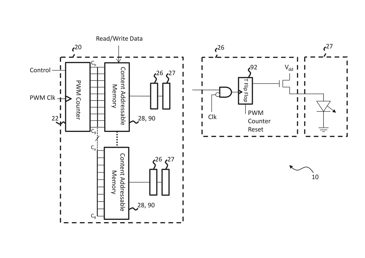
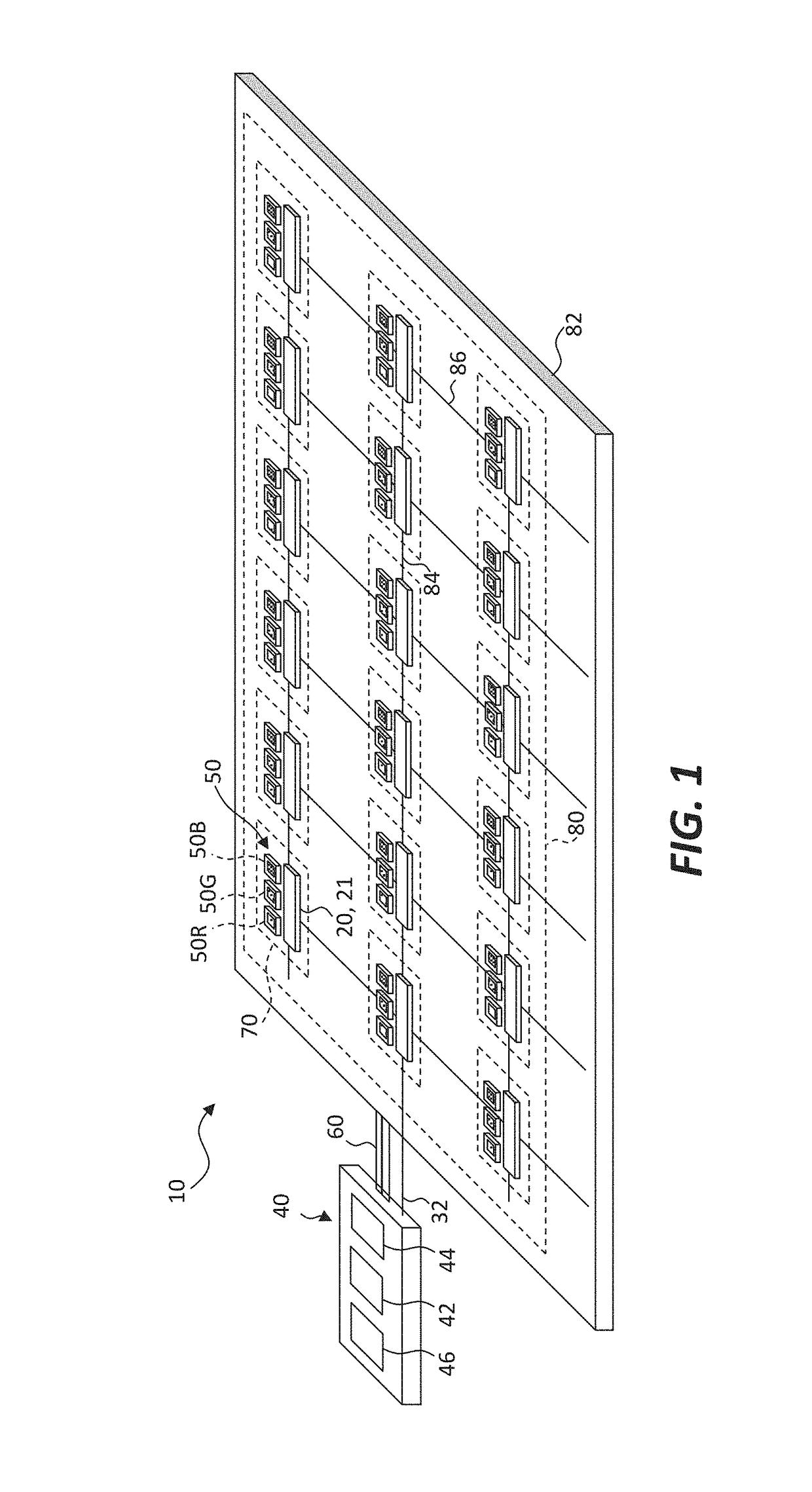
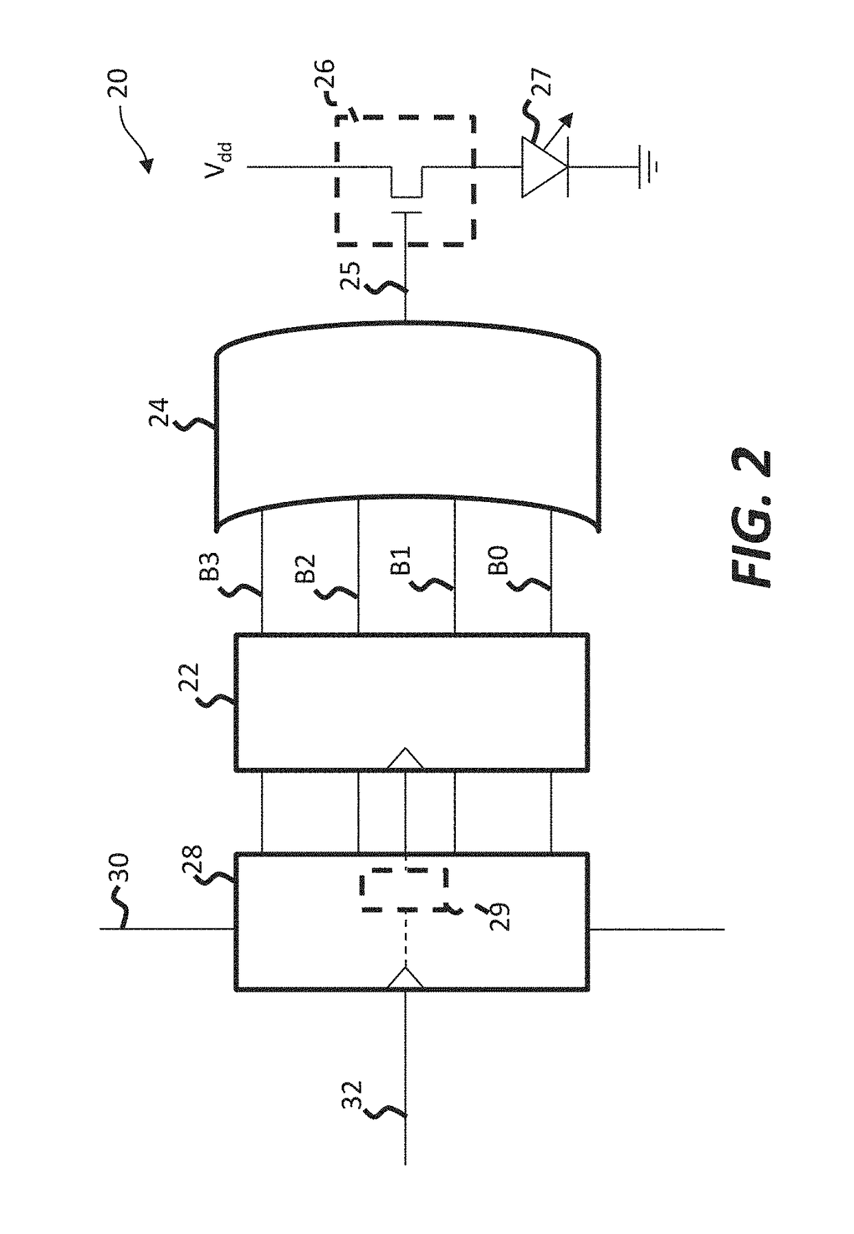
[0069]Referring to the perspective illustration of FIG. 1 and the corresponding detailed schematic of FIG. 2, according to an exemplary embodiment of the present invention a distributed pulse-width modulation system 10 includes an array of pulse-width modulation elements 20. In some embodiments, the array of pulse-width modulation elements 20 is spatially distributed over a system substrate 82 in rows and columns. Each element 20 includes a digital memory 28 for storing a multi-bit digital value and a drive circuit 26 that drives an output device 27 in response to the multi-bit digital value stored in the digital memory 28. A system controller 40 includes a memory 42 for storing a multi-bit digital value for each element 20 and a communication circuit 44 for communicating each multi-bit digital value to each corresponding pulse-width modulation element 20, for example through a bus 60 electrically connecting the system controller 40 to the elements 20.

[0070]The system controller 40 ...


PUM


Abstract

A distributed pulse-width modulation system includes an array of pulse-width modulation elements, each element including a digital memory for storing a plurality of multi-bit digital values, a drive circuit for each stored multi-bit digital value, and an output device for each stored multi-bit digital value. The multi-bit digital values all have the same number of bits. For each stored multi-bit digital value, the corresponding drive circuit drives the corresponding output device in response to the multi-bit digital value stored in the digital memory. A system controller includes a memory for storing the multi-bit digital values for each pulse-width modulation element and a communication circuit communicates each multi-bit digital value to each corresponding pulse-width modulation element.

Description

PRIORITY APPLICATION[0001]This application claims priority to and benefit of U.S. Patent Application No. 62 / 334,351, filed May 10, 2016, entitled Multi-Pixel Distributed Pulse Width Modulation Control, the content of which is hereby incorporated by reference in its entirety.CROSS REFERENCE TO RELATED APPLICATIONS[0002]Reference is made to commonly assigned U.S. patent application Ser. No. 14 / 835,282, filed Aug. 25, 2015, entitled Bit-Plane Pulse Width Modulated Digital Display System by Cok et al., the disclosure of which is incorporated herein by reference in its entirety.FIELD OF THE INVENTION[0003]The present invention relates to systems using digital values driven by pulse-width modulation.BACKGROUND OF THE INVENTION[0004]Flat-panel displays are widely used in conjunction with computing devices, in portable devices, and for entertainment devices such as televisions. Such displays typically employ a plurality of pixels distributed over a display substrate to display images, graph...

Claims


Application Information

Patent Timeline
IPC IPC(8): G09G3/3225
CPCG09G3/3225G09G2320/064G09G2300/0857G09G2310/0286G09G2310/08G09G2310/061G09G3/2014
Inventor COK, RONALD S.ROTZOLL, ROBERT R.
Owner X DISPLAY CO TECH LTD
Learn More