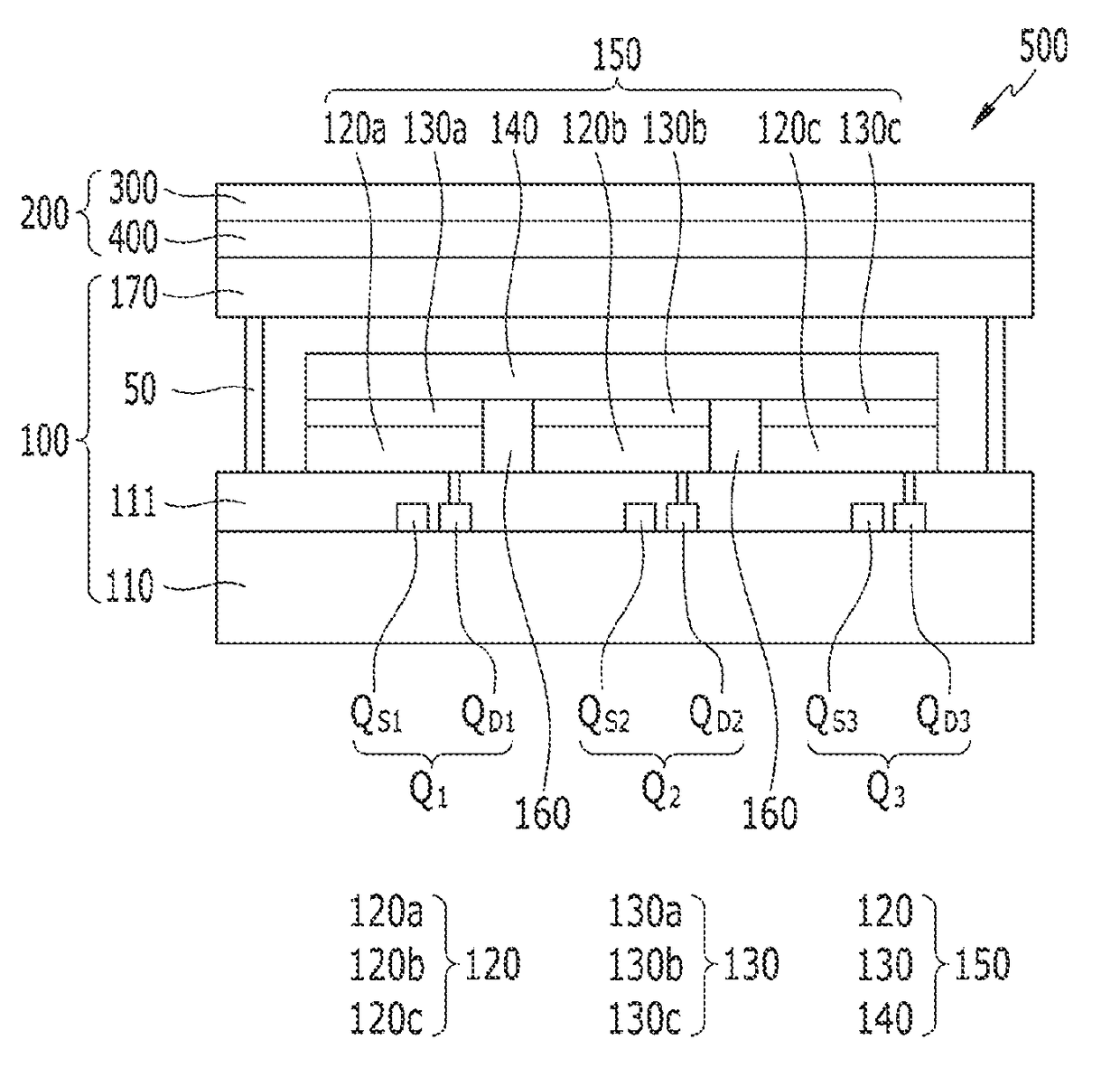
Organic light emitting diode device
a light-emitting diode and organic technology, applied in the direction of diodes, polarising elements, instruments, etc., can solve the problems of deteriorating display quality and the use of organic light-emitting diodes, and achieve the effect of reducing external light reflection and reducing external light emission
- Summary
- Abstract
- Description
- Claims
- Application Information
AI Technical Summary
Benefits of technology
Problems solved by technology
Method used
Image

Examples
preparation example 1
[0290]A commercially available polycarbonate film R-140 (a λ / 4 retardation film, Kaneka Corp.) is used as a first compensation film.
[0291]In addition, vertically-aligned liquid crystals are spin-coated on a non-elongated polycarbonate film and pre-cured. Subsequently, the liquid crystals are cured by radiating a light of ultra-violate (“UV”) 500 millijoules (mJ) to prepare a second compensation film including a liquid crystal layer having refractive indices satisfying the following inequation: nz2>nx2=ny2. Then, a first compensation film and a second compensation film are bonded by using a pressure sensitive adhesive (“PSA”) to prepare a compensation film. Then, a polarizing plate (SEG1425DU, Nitto Denko Co. Ltd.) is adhered to the first compensation film to manufacture a circular polarizing plate.
[0292]The second compensation film has a retardation provided in Table 1, and the retardation is measured by using an Axoscan equipment (Axometrics Inc.) within a wavelength ranging from 4...
preparation examples 2 to 6
[0293]Each circular polarizing plate is manufactured according to the same method as Preparation Example 1 except for preparing a second compensation film having a different retardation as shown in Table 1 by changing the spin speed of spin-coating liquid crystals.
TABLE 1Thickness directionIn-plane retardationretardation(Re2, nm) (@ 550 nm)(Rth2, nm) (@ 550 nm)Preparation Example 1−62Preparation Example 2−85Preparation Example 3−98Preparation Example 4−122Preparation Example 5−133Preparation Example 6−140
Manufacture of Organic Light-Emitting Diode Device
examples 1 to 6
[0294]Each organic light emitting diode device is manufactured by respectively attaching the circular polarizing plates according to Preparation Examples 1 to 6 to an organic light emitting display panel (Galaxy S4 Panel, Samsung Display).
PUM
 Abstract
Description
Claims
Application Information
 - R&D
- Intellectual Property
- Life Sciences
- Materials
- Tech Scout
- Unparalleled Data Quality
- Higher Quality Content
- 60% Fewer Hallucinations
Browse by: Latest US Patents, China's latest patents, Technical Efficacy Thesaurus, Application Domain, Technology Topic, Popular Technical Reports.
© 2025 PatSnap. All rights reserved.Legal|Privacy policy|Modern Slavery Act Transparency Statement|Sitemap|About US| Contact US: help@patsnap.com