
Capacitive in-cell touch panel and display device

a display device and capacitive in-cell technology, applied in the field of capacitive in-cell touch panel and display device, can solve the problems of low light transmittance, high manufacturing cost, and suffer from add-on mode touch panel, and achieve the effect of enhanced touch sensitivity

Active Publication Date: 2016-11-24
SHENZHEN CHINA STAR OPTOELECTRONICS TECH CO LTD
View PDF2 Cites 6 Cited by
  • Summary
  • Abstract
  • Description
  • Claims
  • Application Information

AI Technical Summary

Benefits of technology

The present invention is a capacitive in-cell touch panel that solves the problem of liquid crystal aperture ratio being affected and improves touch reliability. It has two capacitive sensors at a touch site, namely a stacked and intersecting first capacitive touch layer and second capacitive touch layer. Each layer uses a conductive layer and signal line to establish capacitive coupling for touch control, leading to enhanced touch sensitivity. The transmitting and receiving lines of each layer are arranged on the black matrix or have an orthogonal projection located on it to avoid blocking an open area that affects aperture ratio.

Problems solved by technology

The add-on mode touch panel suffers various disadvantages, such as high manufacturing cost, low light transmittance, and large module thickness.
Heretofore, the in-cell touch panel that is currently known is made by directly adding a capacitive sensor and touch wires on a thin-film transistor (TFT) array substrate; however, adding the capacitive sensor and the touch wires on a conventional TFT array substrate affects the aperture ratio of the TFT array and touch sensitivity and thus reducing the reliability of the touch operation.

Method used


Image

  • Capacitive in-cell touch panel and display device
  • Capacitive in-cell touch panel and display device
  • Capacitive in-cell touch panel and display device

Examples


Embodiment Construction

[0024]A clear and complete description will be given to technical solutions of the embodiments of the present invention with reference to the attached drawings of the embodiments of the present invention.

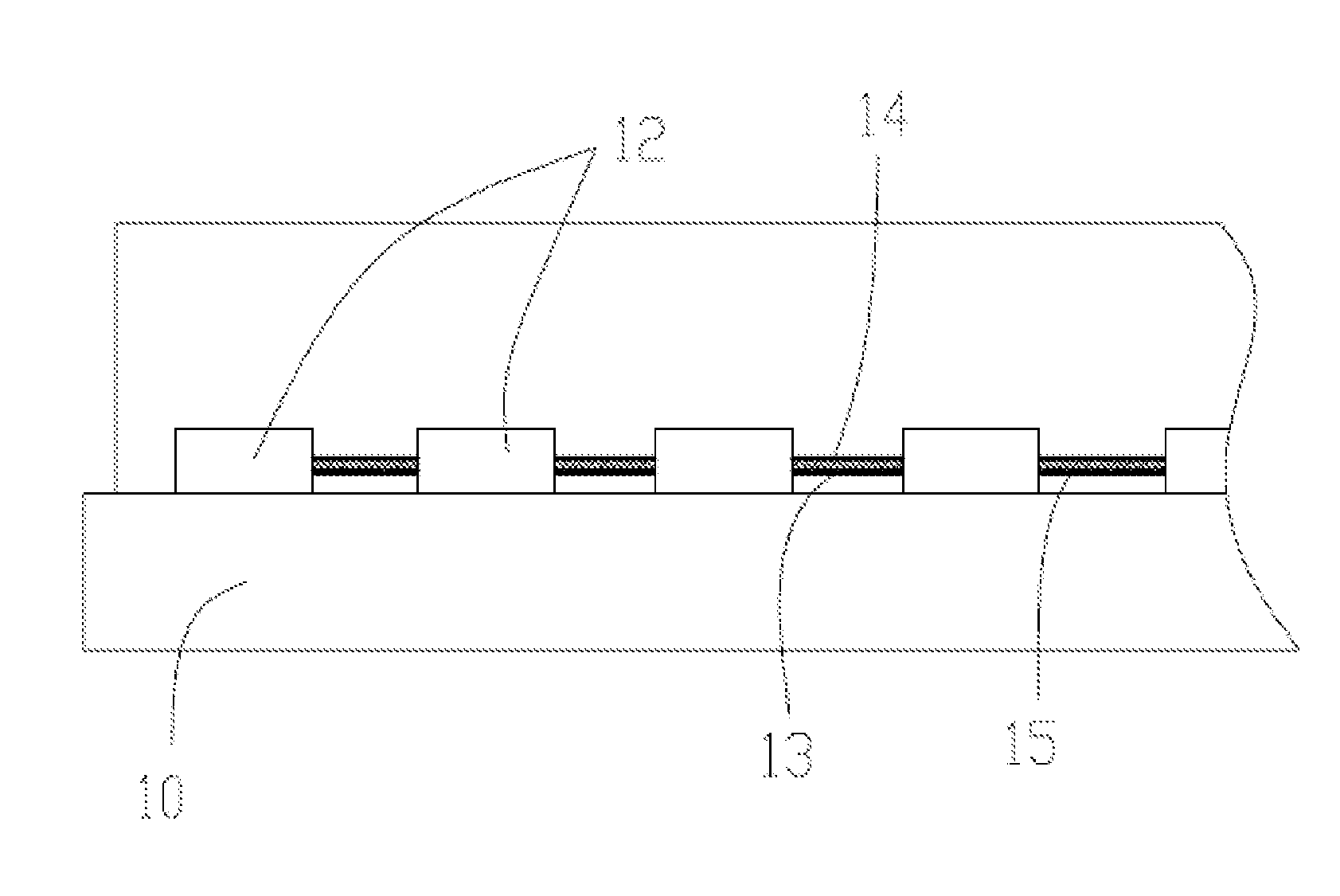
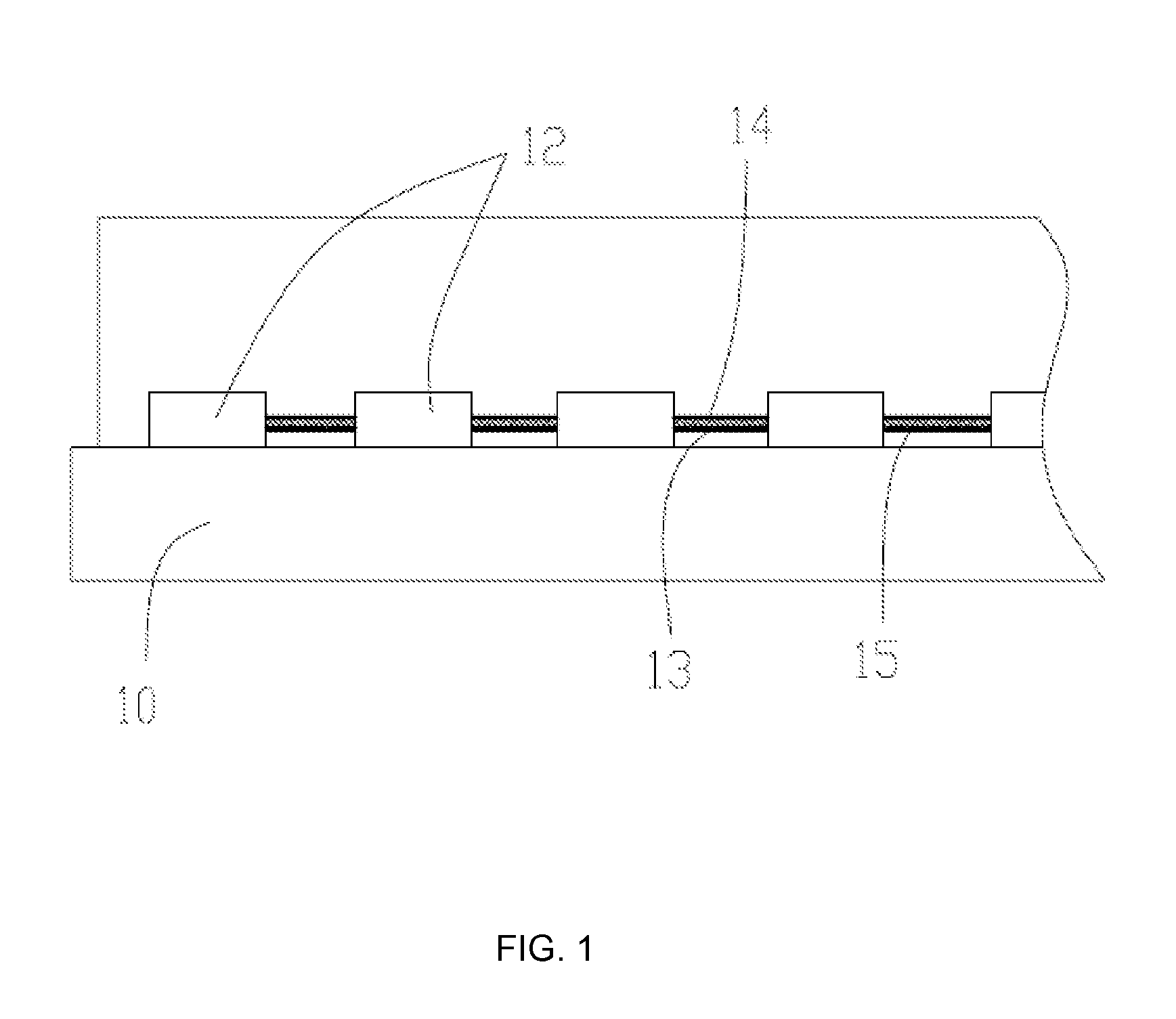
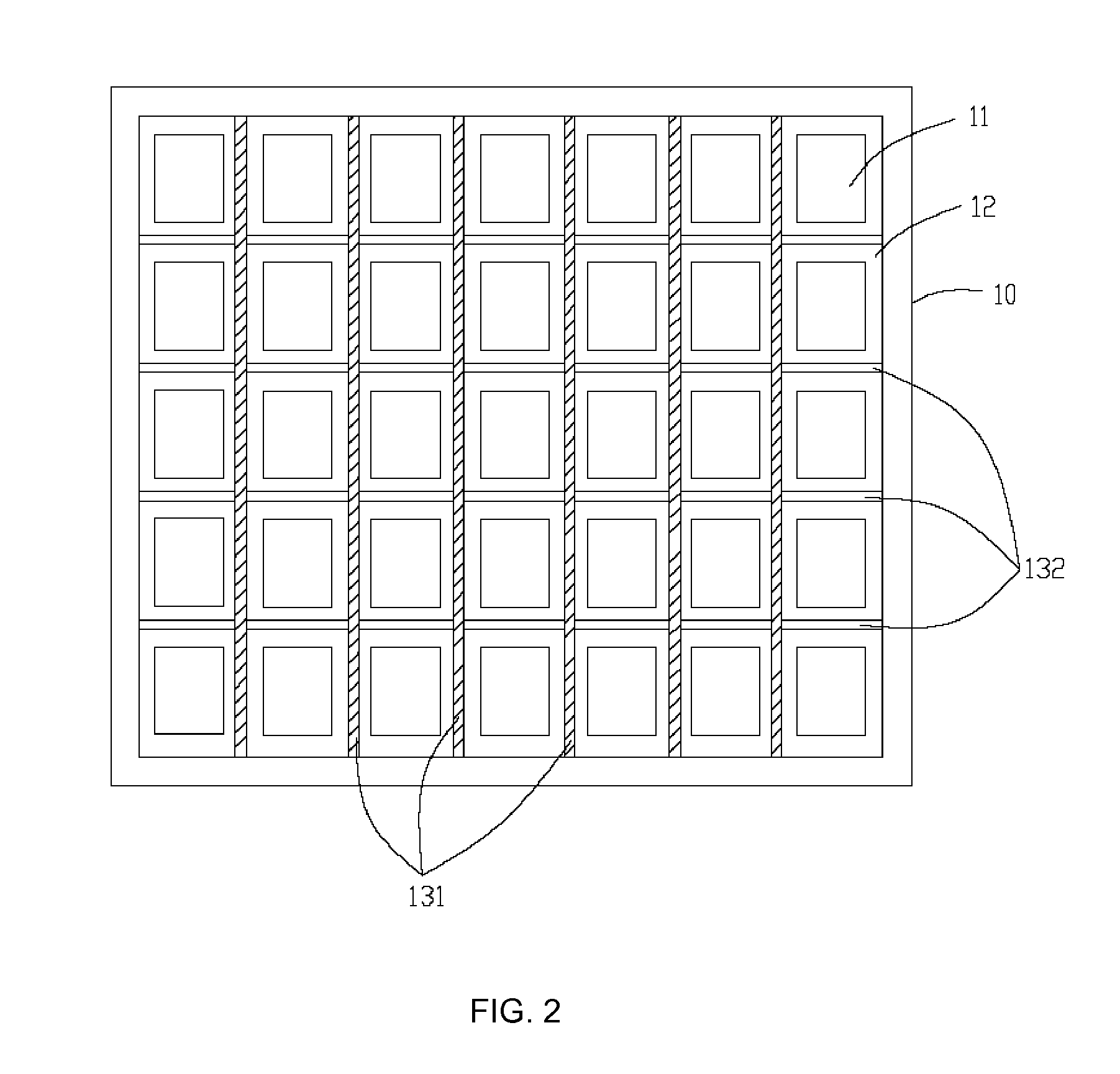
[0025]Referring to FIGS. 1 and 2, a preferred embodiment of the present invention provides a capacitive in-cell touch panel, which comprises a substrate 10 and a black matrix 12 disposed on the substrate 10. The capacitive in-cell touch panel further comprises a first capacitive touch layer 13 and a second capacitive touch layer 14. The first capacitive touch layer 13 and the second capacitive touch layer 14 are formed on the black matrix 12 to be stacked on and intersecting each other in a grid form. Further, the first capacitive touch layer 13 and the second capacitive touch layer 14 are isolated from each other by arranging an insulation layer 15 therebetween.

[0026]In an embodiment, the substrate 10 is a glass panel with a color filtering function. A liquid crystal panel of a thi...


PUM


Abstract

Disclosed is a capacitive in-cell touch panel, which includes a substrate and a black matrix disposed on the substrate. The capacitive in-cell touch panel further includes a first capacitive touch layer, an insulation layer, and a second capacitive touch layer. The first capacitive touch layer is formed on the black matrix. The insulation layer is formed on the first capacitive touch layer. The second capacitive touch layer is formed on the second capacitive touch layer and is stacked on and intersects the first capacitive touch layer in a grid form. Also disclosed is a display device.

Description

CROSS REFERENCE TO RELATED APPLICATIONS[0001]This application claims the priority of Chinese Patent Application No. 201410667531.6, entitled “Capacitive In-Cell Touch Panel and Display Device”, filed on Nov. 20, 2014, the disclosure of which is incorporated herein by reference in its entirety.BACKGROUND OF THE INVENTION[0002]1. Field of the Invention[0003]The present invention relates to the field of liquid crystal displaying technology, and in particular to a capacitive in-cell touch panel and a display device.[0004]2. The Related Arts[0005]With the fast progress of the displaying technology, touch screen panels have been widely prevailing in the living of people. Currently, the touch screen panels are classified, according to the structure thereof, into add-on mode touch panels, on-cell touch panel, and in-cell touch panel. The add-on mode touch panels are made by separately manufacturing a touch panel and a liquid crystal display (LCD) that are then laminated together to form a l...

Claims


Application Information

Patent Timeline
IPC IPC(8): G06F3/044G02F1/1333G02F1/1362G06F3/041
CPCG06F3/044G06F3/0412G06F3/0418G06F2203/04107G02F1/136209G06F2203/04111G02F1/13338G06F3/0445G06F3/0446G06F2203/04103
Inventor XU, XIANGYANG
Owner SHENZHEN CHINA STAR OPTOELECTRONICS TECH CO LTD
Learn More