Compensation Circuit, Amoled Structure and Display Device

a technology of amoled structure and compensation circuit, applied in the field of compensating circuit, amoled structure and display device, can solve the problems of 100/b> occupying more space, and being conducive to the design of narrow border products

Active Publication Date: 2016-10-27
EVERDISPLAY OPTRONICS (SHANGHAI) CO LTD
View PDF3 Cites 1 Cited by
  • Summary
  • Abstract
  • Description
  • Claims
  • Application Information

AI Technical Summary

Benefits of technology

[0011]a signal control terminal configured to output a predetermined signal after the second pixel unit goes through the anode initialization state, the CST initialization state and the data inputting state, to cause the light emitter to operate in a light-emitting state.

Problems solved by technology

In addition, as the control terminal processes too much data, the circuit 100 begins to take up more space during the connection process, which is not conducive to the design of narrow border products.

Method used


Image

  • Compensation Circuit, Amoled Structure and Display Device
  • Compensation Circuit, Amoled Structure and Display Device
  • Compensation Circuit, Amoled Structure and Display Device

Examples


Embodiment Construction

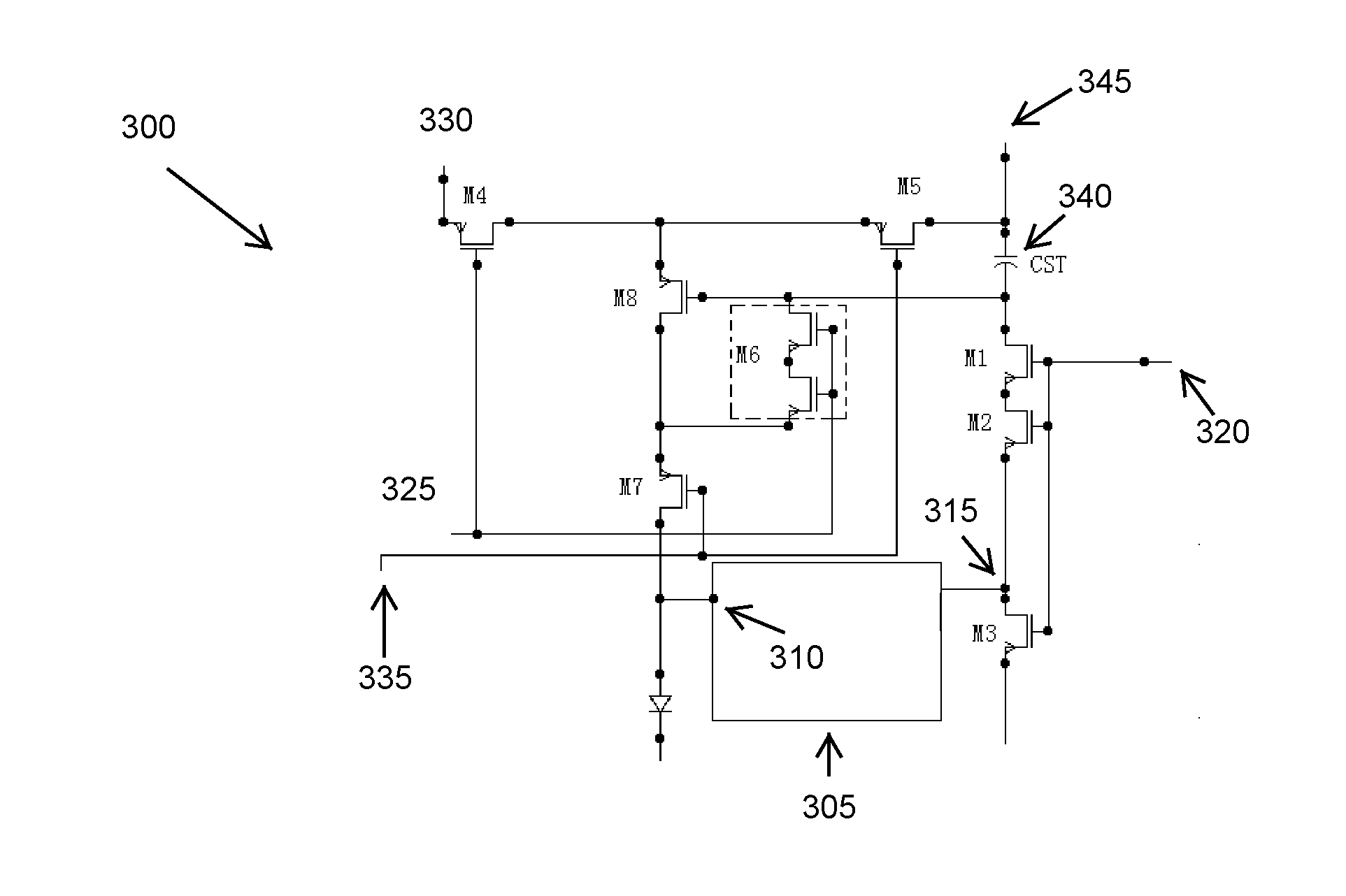
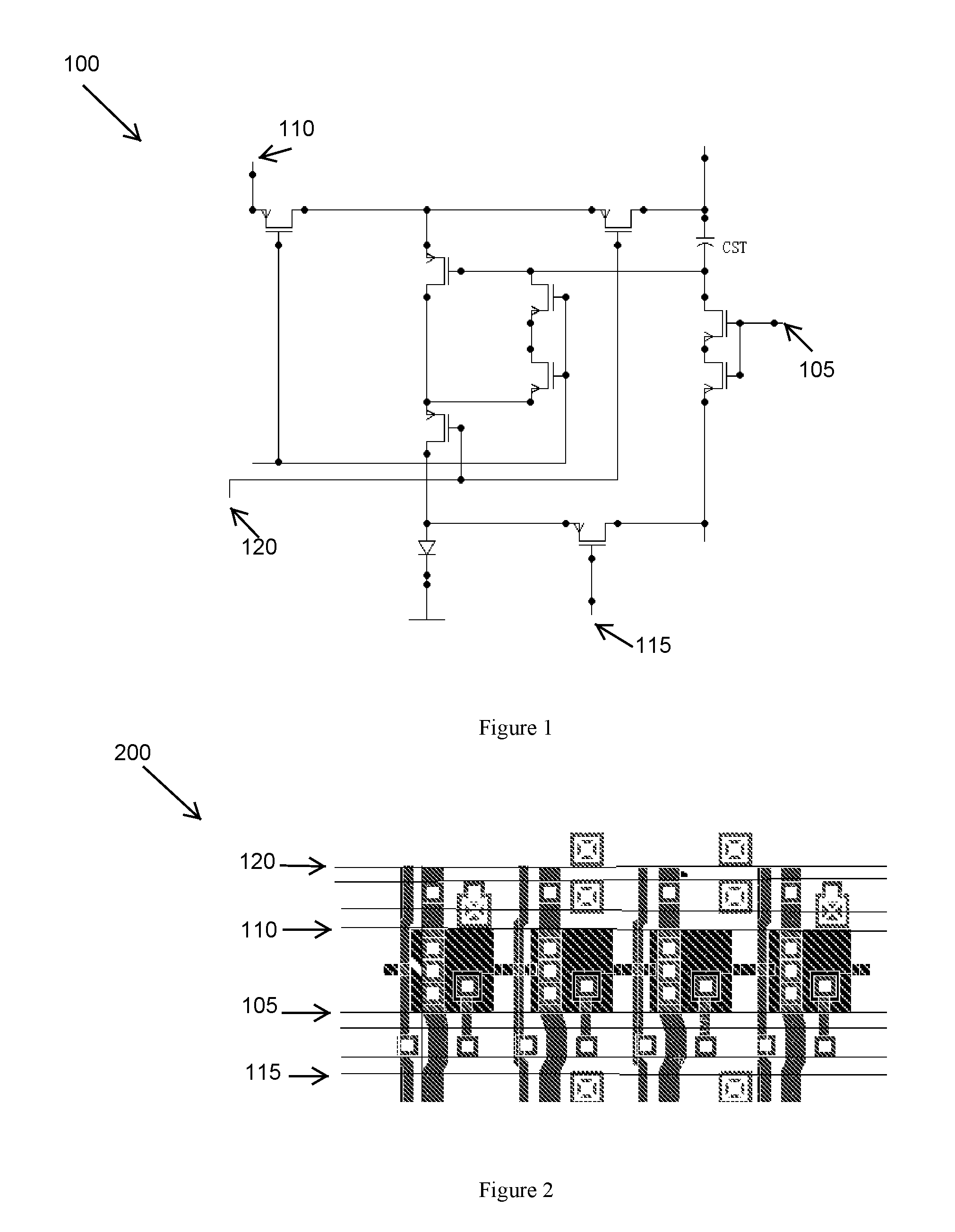
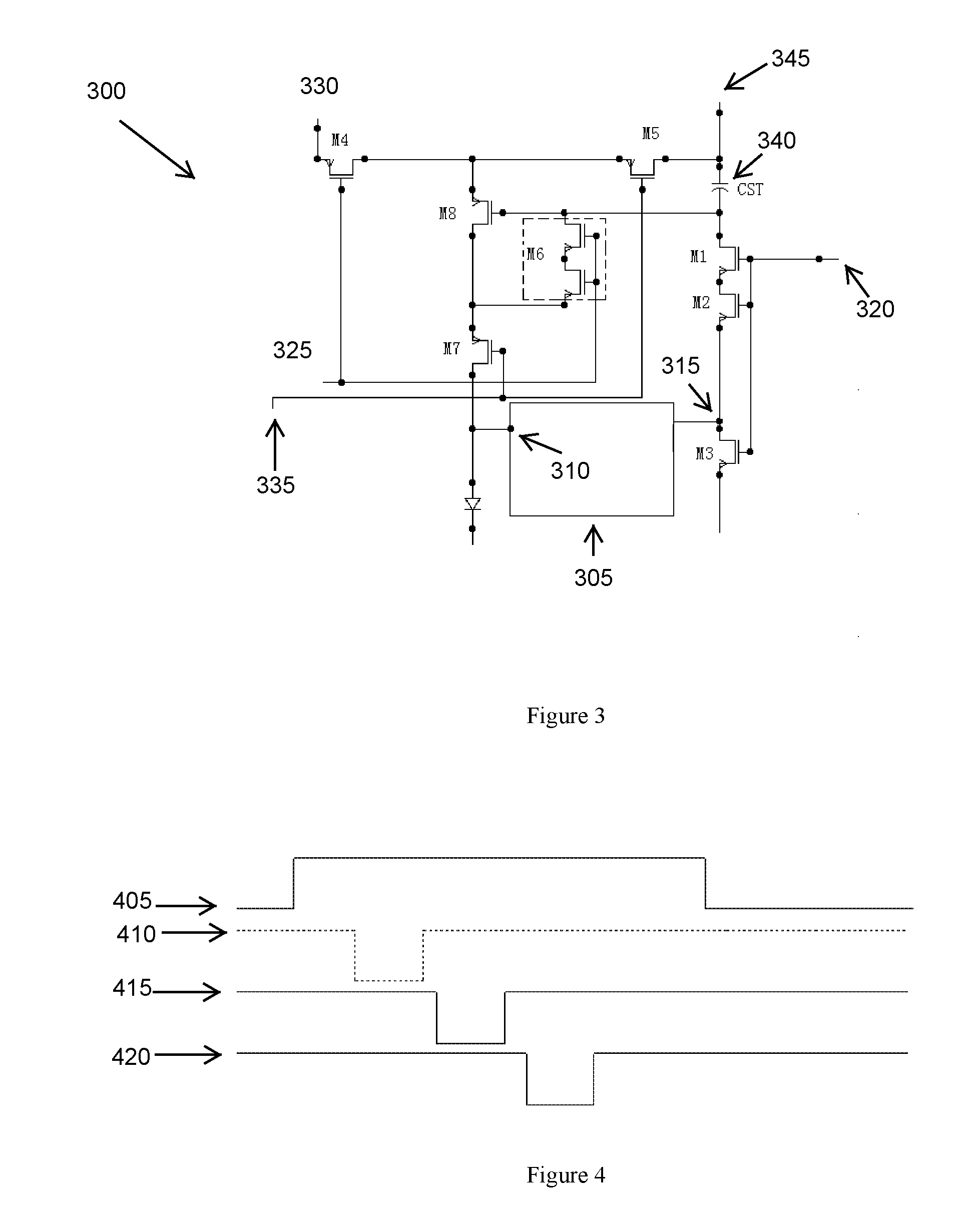
[0047]The present invention will now be described more fully hereinafter with reference to the accompanying drawings, in which exemplary embodiments of the invention are shown. This invention may, however, be embodied in many different forms and should not be construed as limited to the embodiments set forth herein. Rather, these embodiments are provided so that this disclosure will be thorough and complete, and will fully convey the scope of the invention to those skilled in the art. Like reference numerals refer to like elements throughout.

[0048]The terminology used herein is for the purpose of describing particular embodiments only and is not intended to be limiting of the invention. As used herein, the singular forms “a”, “an” and “the” are intended to include the plural forms as well, unless the context clearly indicates otherwise. It will be further understood that the terms “comprises” and / or “comprising,” or “includes” and / or “including” or “has” and / or “having” when used he...


PUM


Abstract

The present invention relates to the field of display apparatus, more specifically, to a compensation circuit, an AMOLED structure and a display device. Said circuit comprises a plurality of pixel units, each for the plurality of pixel units includes at least one light emitter, and each of said pixel units comprises: an anode initialization signal interface, a CST initialization port, a data control port and an enable signal control port. Compared with the prior art, the advantages of the present invention are: according to the invention, there is no need to individually set up an anode initialization signal line, the umber of the signal lines are reduced from 4 to 3, which is benefit for achieving the design of the product HPPI. And the signal control lines reduce the space occupied by jumper wire during the connection process, which is benefit to the design of narrow border products.

Description

[0001]The present application claims priority to and the benefit of Chinese Patent Application No. CN 201510197799.2, filed on Apr. 23, 2015, the entire content of which is incorporated herein by reference.FIELD OF THE INVENTION[0002]The invention relates to the field of display apparatus, more specifically, to a compensation circuit, an AMOLED structure and a display device.BACKGROUND OF THE INVENTION[0003]As shown in FIG. 1, the conventional pixel compensation circuit 100 is normally provided with, in addition to a power terminal, four signal control terminals: Storage Capacitance (CST) initialization terminal 105, data input terminal 110, anode initialization terminal 115, and control terminal 120. Such a pixel compensation circuit has four different operating states—they are CST initialization state, data inputting state, anode initialization state, and light-emitting state, respectively. At first, the capacitor is charged when the circuit 100 operates in the CST initialization ...

Claims


Application Information

Patent Timeline
Patent Type & Authority Applications(United States)
IPC IPC(8): G09G3/3258
CPCG09G3/3258G09G2300/0819G09G2300/0439G09G3/30G09G2300/0426G09G2300/0814G09G2300/0842G09G2300/0861G09G2310/0262G09G2310/08
Inventor XIONG, NANAFENG, YU-HSIUNGWANG, JIANGANG
Owner EVERDISPLAY OPTRONICS (SHANGHAI) CO LTD
Why Eureka
Try Eureka