
Display device

a technology of display device and display screen, which is applied in the field of display device, can solve the problems of deteriorating display quality, increasing luminance, and increasing power consumption of backlight, and achieves the effects of reducing power consumption, improving luminance, and reducing current value of backligh

Active Publication Date: 2015-12-03
JAPAN DISPLAY INC
View PDF5 Cites 6 Cited by
  • Summary
  • Abstract
  • Description
  • Claims
  • Application Information

AI Technical Summary

Benefits of technology

The patent describes a display device that reduces power consumption and noise by adding a white pixel to the red, green, and blue sub-pixels of a pixel. This is achieved by performing column inversion driving, which alternates the polarities of voltages applied to the sub-pixels. The display device also includes a modification that alternately arranges the sub-pixels of different colors in the row and column directions to increase luminance and achieve wider color representation. These modifications result in improved display quality and reduced power consumption.

Problems solved by technology

An increase of the luminance of a backlight increases power consumption of backlight.
In such a configuration, however, although a pixel area can be prevented from being increased and high definition can be achieved even when the fourth sub-pixel is added, deterioration in display quality called crosstalk may be caused when the technique disclosed in Japanese Examined Patent Application Publication No.

Method used


Image

  • Display device
  • Display device
  • Display device

Examples


first modification

[0143]FIG. 22 is a conceptual diagram of the image display panel of the display device according to a first modification of the embodiment. In the pixels 48A and the pixels 48B of the image display panel 30, the first sub-pixel columns in which the first sub-pixels 49W of white are arranged, the second sub-pixel columns arranged next to the respective first sub-pixel columns in which the second sub-pixels 49G of green are arranged, and the third sub-pixel columns arranged next to the respective second sub-pixel columns are repeatedly arranged. The third sub-pixels 49B of blue and the fourth sub-pixels 49R of red are alternately arranged in the row direction across the third sub-pixel columns, and the third sub-pixels 49B and the fourth sub-pixels 49R are alternately arranged in the column direction in the same column of the third sub-pixel columns. Voltages applied to the first sub-pixel columns to the third sub-pixel columns are the same as the example illustrated in FIG. 17. With ...

second modification

[0144]FIG. 23 is a diagram illustrating the pixel array of the image display panel of the display device according to a second modification of the embodiment. In the pixels 48A and the pixels 48B of the image display panel 30, the first sub-pixel columns in which the first sub-pixels 49R of red are arranged, the second sub-pixel columns arranged next to the respective first sub-pixel columns in which the second sub-pixels 49G of green are arranged, and the third sub-pixel columns arranged next to the respective second sub-pixel columns are repeatedly arranged. The third sub-pixels 49B of blue and fourth sub-pixels 49Y of yellow are alternately arranged in the row direction across the third sub-pixel columns, and the third sub-pixels 49B and the fourth sub-pixels 49Y are alternately arranged in the column direction in the same column of the third sub-pixel columns. For example, a yellow color filter is arranged between the fourth sub-pixel 49Y and an image observer. Voltages applied ...

application examples

4. Application Examples

[0152]The following describes application examples of the present disclosure in which the display device 10 described above is applied to electronic apparatuses.

[0153]FIGS. 26 to 38 are diagrams illustrating examples of an electronic apparatus including the display device according to the embodiment. The display device 10 according to the embodiment can be applied to electronic apparatuses in various fields such as a television apparatus, a digital camera, a notebook-type personal computer, a portable electronic apparatus such as a cellular telephone, or a video camera. In other words, the display device 10 can be applied to electronic apparatuses in various fields that display a video signal input from the outside or a video signal generated inside as an image or a video.


PUM


Abstract

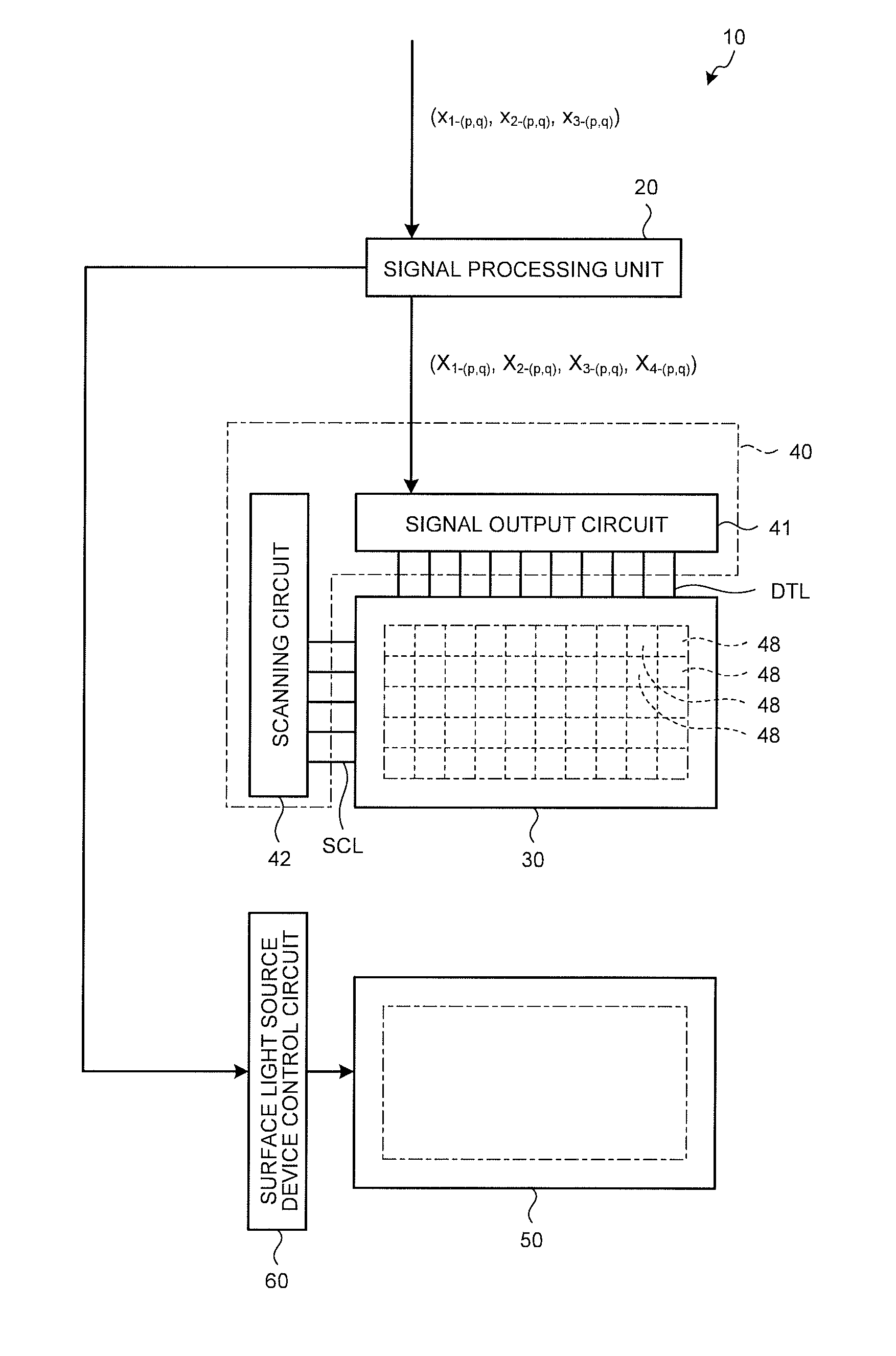
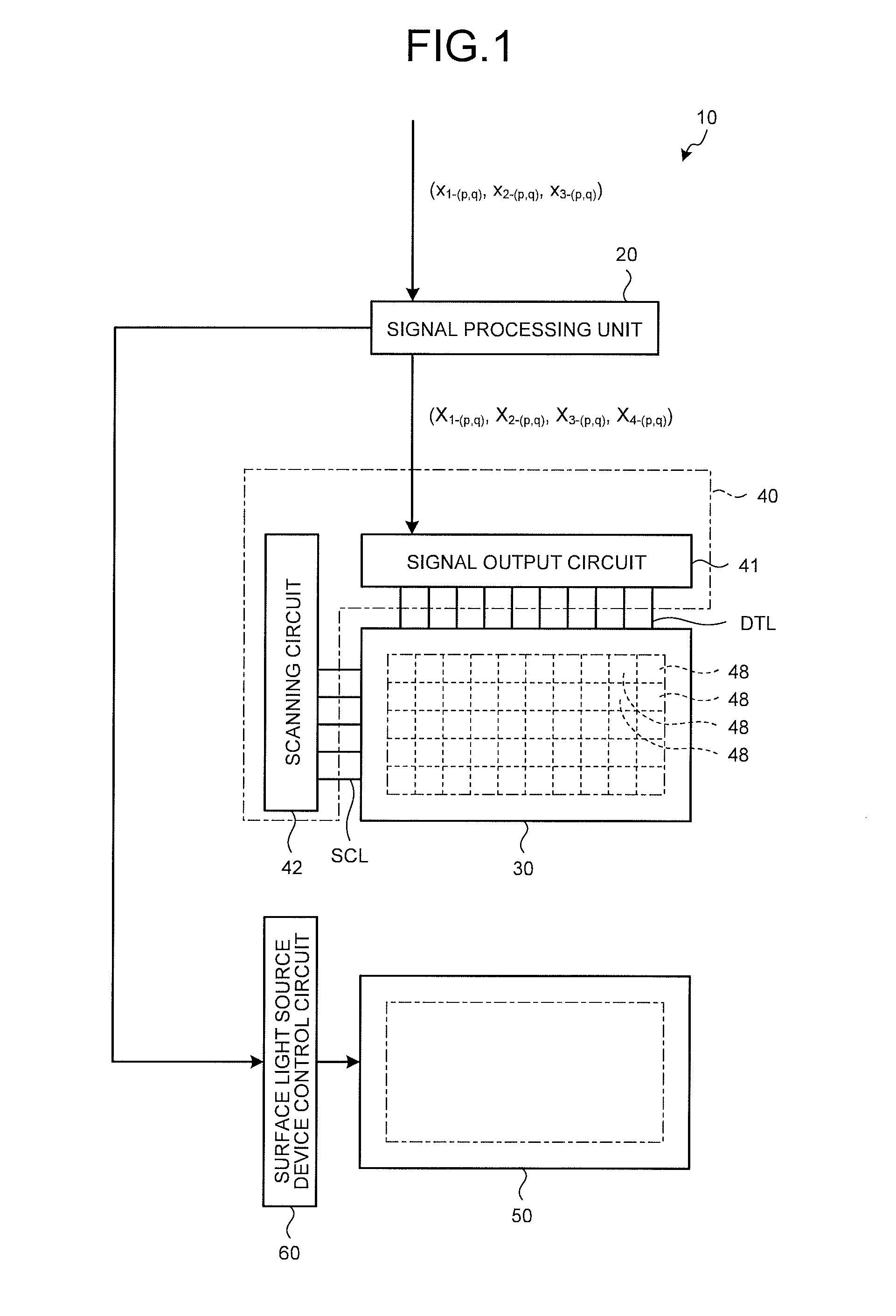
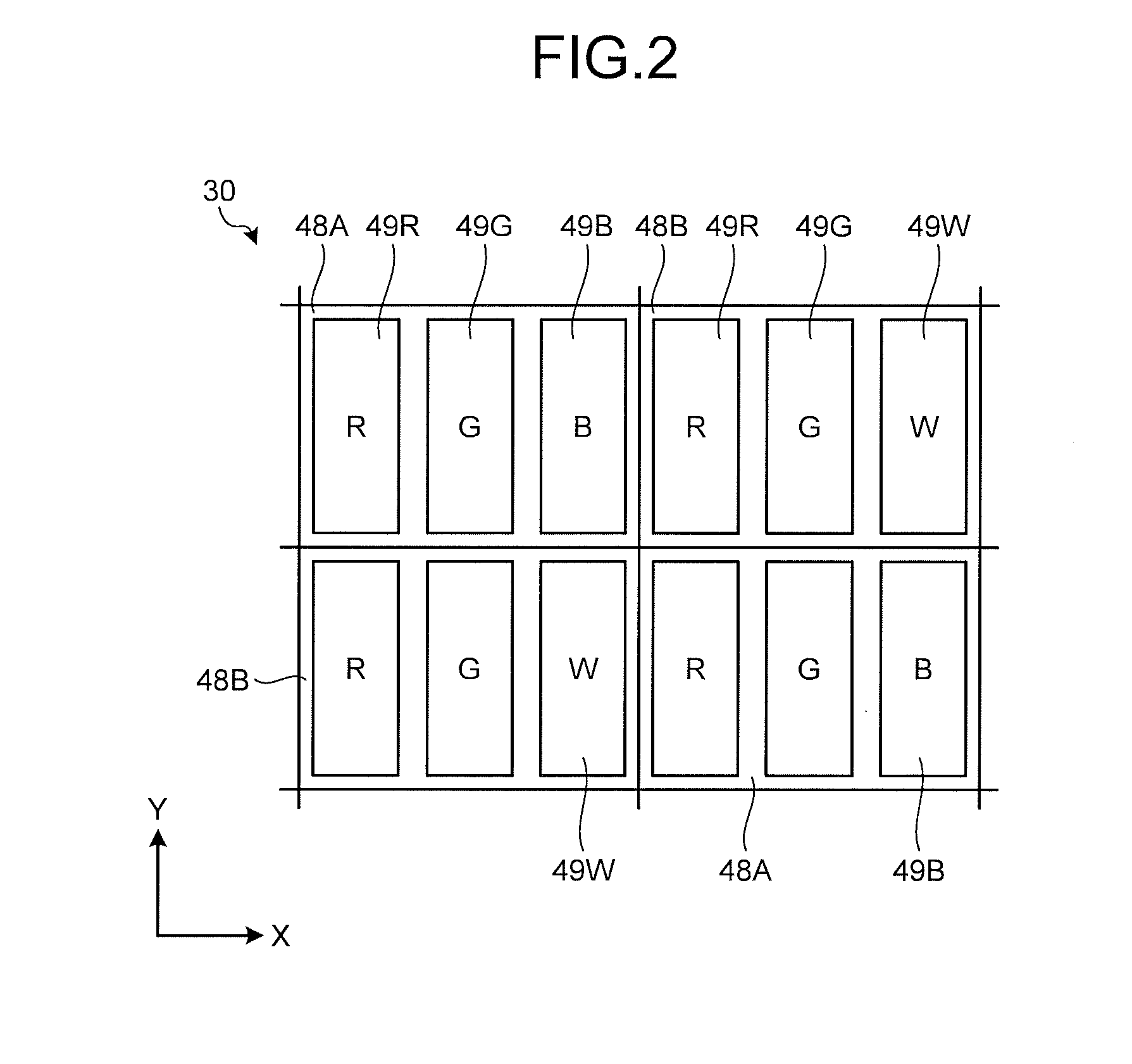
A display device includes an image display panel and a control device. The image display panel includes first sub-pixels, second sub-pixels, third sub-pixels, and fourth sub-pixels in which a specified sub-pixel column including the third sub-pixels and the fourth sub-pixels and at least one other sub-pixel column arranged next to the specified sub-pixel column are periodically arranged. The control device performs column inversion driving to apply a voltage having the same polarity to signal lines of a first specified sub-pixel column belonging to the specified sub-pixel columns and the other sub-pixel column adjacent to the first specified sub-pixel column, apply a voltage having the same polarity as the first specified sub-pixel column to one of the signal lines of a second specified sub-pixel column and a third specified sub-pixel column adjacent to the first specified sub-pixel column, and invert the polarities of the voltages to be applied at predetermined cycles.

Description

CROSS-REFERENCE TO RELATED APPLICATIONS[0001]This application claims priority from Japanese Application No. 2014-115175, filed on Jun. 3, 2014, the contents of which are incorporated by reference herein in its entirety.BACKGROUND[0002]1. Technical Field[0003]The present disclosure relates to a display device.[0004]2. Description of the Related Art[0005]In recent years, demand has been increased for display devices, for example, for mobile apparatuses such as a cellular telephone and electronic paper. In such display devices, each one pixel includes a plurality of sub-pixels that output different colors. Various colors are displayed using the single pixel by switching on and off display at the sub-pixels. Display characteristics such as resolution and luminance have been improved year after year in such display devices. However, an aperture ratio is reduced as the resolution increases, so that luminance of a backlight needs to be increased to achieve high luminance. An increase of th...

Claims


Application Information

Patent Timeline
Patent Type & Authority Applications(United States)
IPC IPC(8): G09G3/36G09G5/18
CPCG09G3/3696G09G2300/0426G09G5/18G09G3/20G09G3/2003G09G3/3614G09G2300/0452G09G2300/0465G09G2330/021G09G2340/0457
Inventor KABE, MASAAKIUCHIYAMA, HIROKIFUKUSHIMA, TOSHIAKIKOIDE, GEN
Owner JAPAN DISPLAY INC
Learn More