Organic electroluminescent element
a technology of electroluminescent elements and organic materials, which is applied in the direction of organic semiconductor devices, thermoelectric devices, solid-state devices, etc., can solve the problems of improving efficiency and problematic fluorescent emission, and achieve the effect of high current density area and efficient white emission
- Summary
- Abstract
- Description
- Claims
- Application Information
AI Technical Summary
Benefits of technology
Problems solved by technology
Method used
Image

Examples
first exemplary embodiment
[0049]FIG. 1 schematically shows an exemplary arrangement of an organic EL device according to a first exemplary embodiment of the invention.
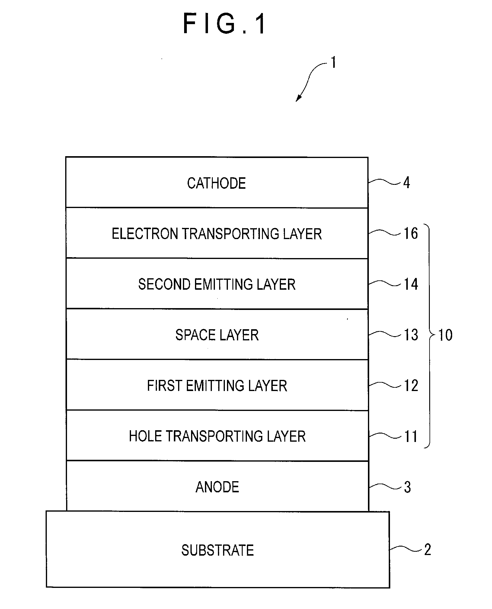
[0050]An organic electroluminescence device 1 includes a light-transmissive substrate 2, an anode 3, a cathode 4 and an organic compound layer 10 disposed between the anode 3 and the cathode 4.
[0051]The organic compound layer 10 has a hole transporting layer 11, first emitting layer 12, space layer 13, second emitting layer 14, and electron transporting layer 16 sequentially from the anode 3. The layers are adjacent to each other.
Emitting Layer
[0052]The organic EL device 1 in the first exemplary embodiment has the first emitting layer 12 and the second emitting layer 14 as the emitting layer. The first emitting layer 12 includes a first host material, second host material, and first dopant material (first luminescent material). The second emitting layer 14 includes a third host material and a second dopant material (second luminescent material)...
second exemplary embodiment
[0234]Next, a second exemplary embodiment is described below.
[0235]In the description of the second exemplary embodiment, the same components as those in the first exemplary embodiment are denoted by the same reference signs and names to simplify or omit an explanation of the components. In the second exemplary embodiment, the same materials and compounds as described in the first exemplary embodiment are usable.
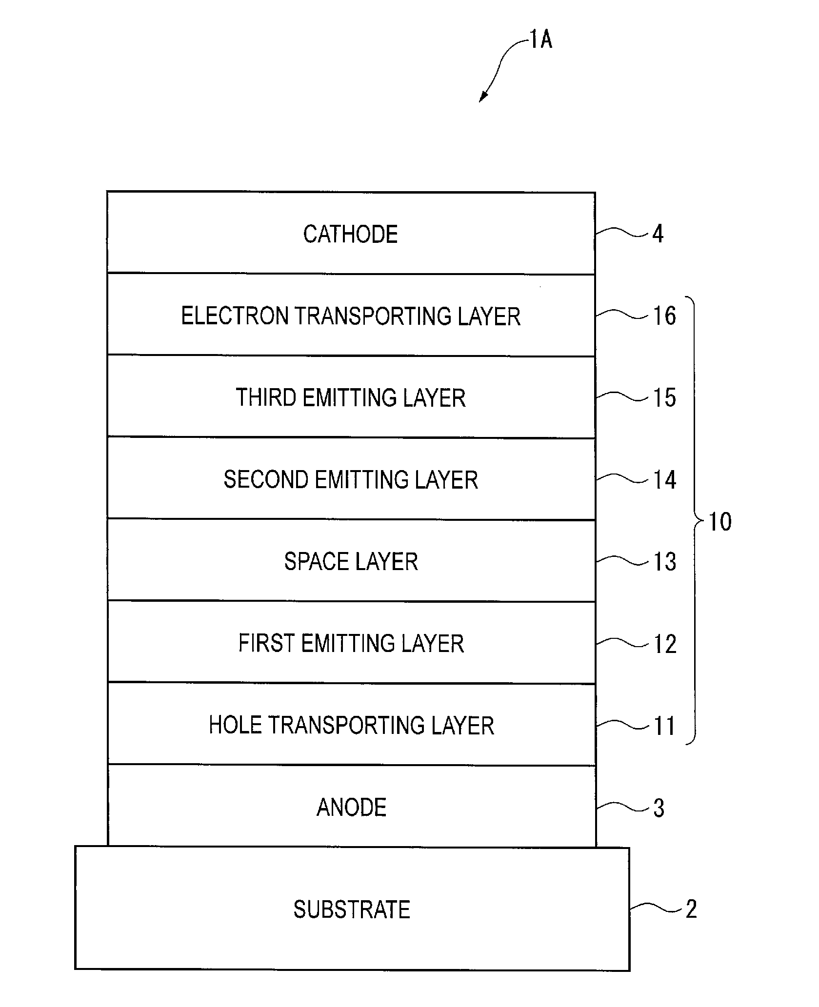
[0236]An organic EL device 1A according to the second exemplary embodiment is different from the organic EL device in the exemplary embodiment in that a third emitting layer 15 is provided adjacent to the second emitting layer 14. As shown in FIG. 9, the anode 3, hole transporting layer 11, first emitting layer 12, space layer 13, second emitting layer 14, third emitting layer 15, electron transporting layer 16, and cathode 4 are laminated on the substrate 2 in this order.
[0237]In the second exemplary embodiment, in order that the organic EL device 1A exhibits a white emissi...
third exemplary embodiment
[0243]Next, a third exemplary embodiment is described below.
[0244]In the description of the third exemplary embodiment, the same components as those in the first exemplary embodiment are denoted by the same reference signs and names to simplify or omit an explanation of the components. In the third exemplary embodiment, the same materials and compounds as described in the first exemplary embodiment are usable.
[0245]An organic EL device 1B in the third exemplary embodiment is different from the organic EL device in the first exemplary embodiment in that no space layer 13 is provided. As shown in FIG. 10, the anode 3, hole transporting layer 11, first emitting layer 12, second emitting layer 14, electron transporting layer 16, and cathode 4 are preferably laminated on the substrate 2 in this order. Moreover, the organic EL device 1B may include the anode 3, hole transporting layer 11, second emitting layer 14, first emitting layer 12, electron transporting layer 16, and cathode 4 whic...
PUM
 Abstract
Description
Claims
Application Information
 - R&D
- Intellectual Property
- Life Sciences
- Materials
- Tech Scout
- Unparalleled Data Quality
- Higher Quality Content
- 60% Fewer Hallucinations
Browse by: Latest US Patents, China's latest patents, Technical Efficacy Thesaurus, Application Domain, Technology Topic, Popular Technical Reports.
© 2025 PatSnap. All rights reserved.Legal|Privacy policy|Modern Slavery Act Transparency Statement|Sitemap|About US| Contact US: help@patsnap.com