Transistor chip and semiconductor device
- Summary
- Abstract
- Description
- Claims
- Application Information
AI Technical Summary
Benefits of technology
Problems solved by technology
Method used
Image


Examples
embodiment 1
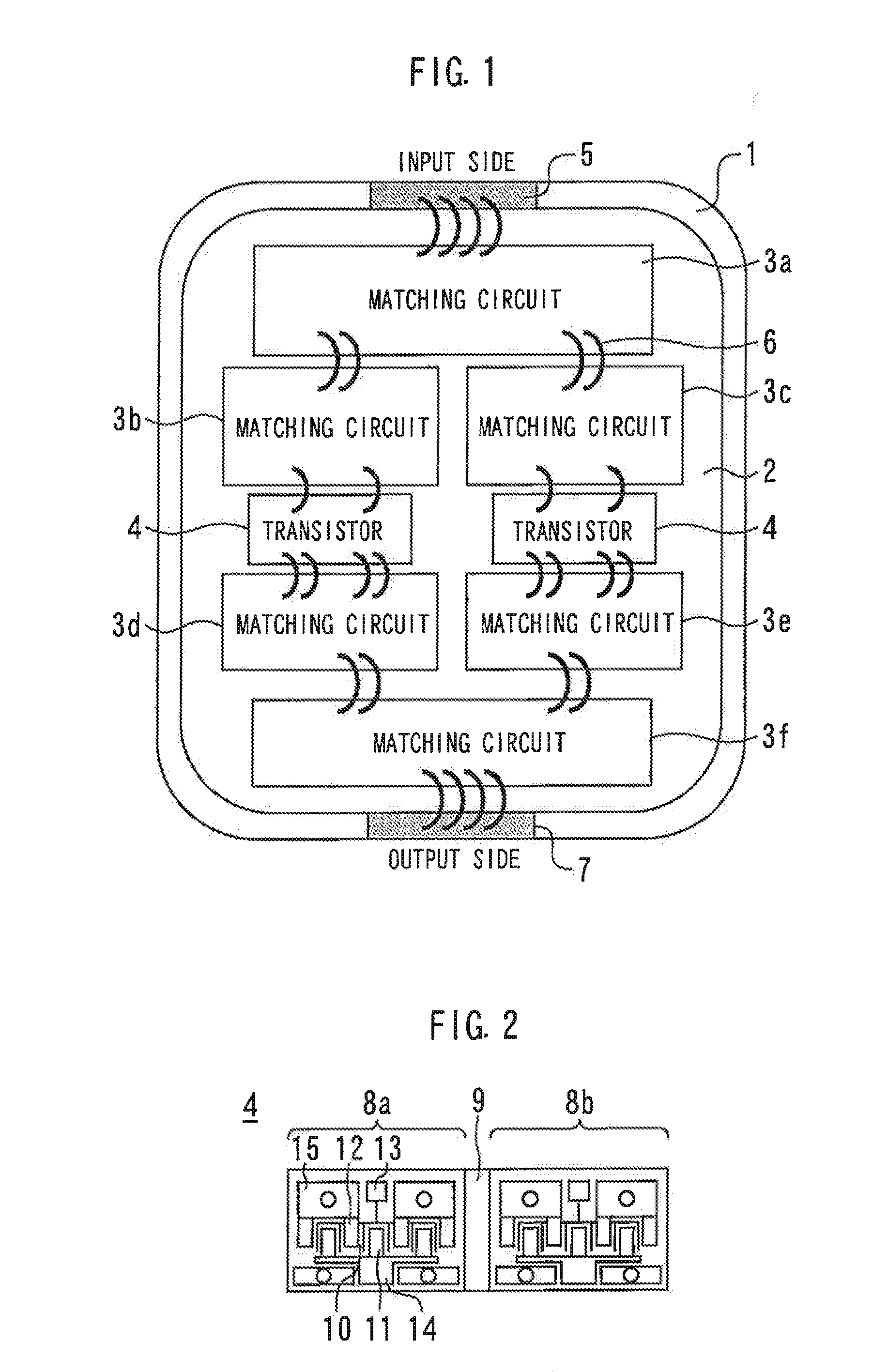
[0019]FIG. 1 is a plan view illustrating a semiconductor device according to Embodiment 1 of the present invention. In a mounted region 2 in a package 1, matching circuits 3a to 3f and a transistor chip 4 are provided. The matching circuits 3a to 3c are connected through wires 6 between an input electrode pad 5 and the transistor chip 4 on the package 1. Matching circuits 3d to 3f are connected between an output electrode pad 7 and the transistor chip 4 on the package 1. This semiconductor device is an internal matching amplifier in which the two transistor chips 4 are connected in parallel.
[0020]FIG. 2 is a plan view illustrating a transistor chip according to Embodiment 1 of the present invention. The transistor chip 4 has two transistor cells 8a and 8b and a separation region 9 for electrically separating operation regions of the transistor cells 8a and 8b from each other. Each of the transistor cells 8a and 8b has a gate electrode 10, a drain electrode 11, a source electrode 12,...
embodiment 2
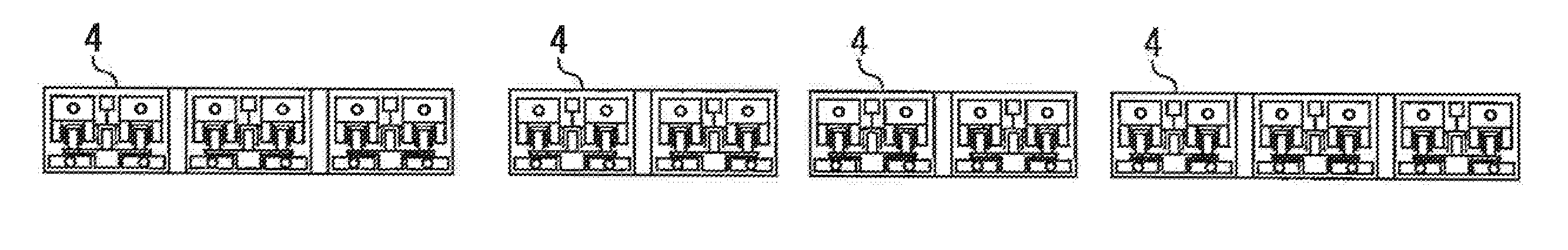
[0026]FIG. 7 is an enlarged plan view of a semiconductor device according to Embodiment 2 of the present invention. Heat generated from the plurality of transistor chips 4 might concentrate on a center part of the mounted region 2.
[0027]Particularly in an internal matching circuit with a large output exceeding 10 W or the like, the number of gate fingers and the number of cells of the transistor chip in use become large (the number of cells to be integrated can be 10 cells or more) and thus, heat concentration to the center part of the mounted region 2 is remarkable.
[0028]On the other hand, in this embodiment, in the plurality of transistor chips 4 juxtaposed on the mounted region 2, an interval W1 of the plurality of transistor chips 4 at the center part of the mounted region 2 is larger than an interval W2 of the plurality of transistor chips 4 in a peripheral part of the mounted region 2. As a result, heat concentration at the center part of the mounted region 2 can be prevented,...
embodiment 3
[0029]FIG. 8 is an enlarged plan view illustrating a semiconductor device according to Embodiment 3 of the present invention. In the plurality of transistor chips 4 juxtaposed on the mounted region 2, the number of transistor cells of the transistor chip 4 at the center part of the mounted region 2 is smaller than the number of transistor cells of the transistor chip 4 in the peripheral part of the mounted region 2. As a result, heat concentration at the center part of the mounted region 2 can be prevented, and heat radiation can be improved.
PUM
 Abstract
Description
Claims
Application Information
 - R&D
- Intellectual Property
- Life Sciences
- Materials
- Tech Scout
- Unparalleled Data Quality
- Higher Quality Content
- 60% Fewer Hallucinations
Browse by: Latest US Patents, China's latest patents, Technical Efficacy Thesaurus, Application Domain, Technology Topic, Popular Technical Reports.
© 2025 PatSnap. All rights reserved.Legal|Privacy policy|Modern Slavery Act Transparency Statement|Sitemap|About US| Contact US: help@patsnap.com