Data processing device and driving method thereof
a technology of data processing and driving method, which is applied in the direction of instruments, computing, climate sustainability, etc., can solve problems such as accidental application of force, and achieve the effects of high operability, low power, and high operability
- Summary
- Abstract
- Description
- Claims
- Application Information
AI Technical Summary
Benefits of technology
Problems solved by technology
Method used
Image
Examples
embodiment 1
[0052]In this embodiment, a structure of a data processing device of one embodiment of the present invention will be described with reference to drawings.
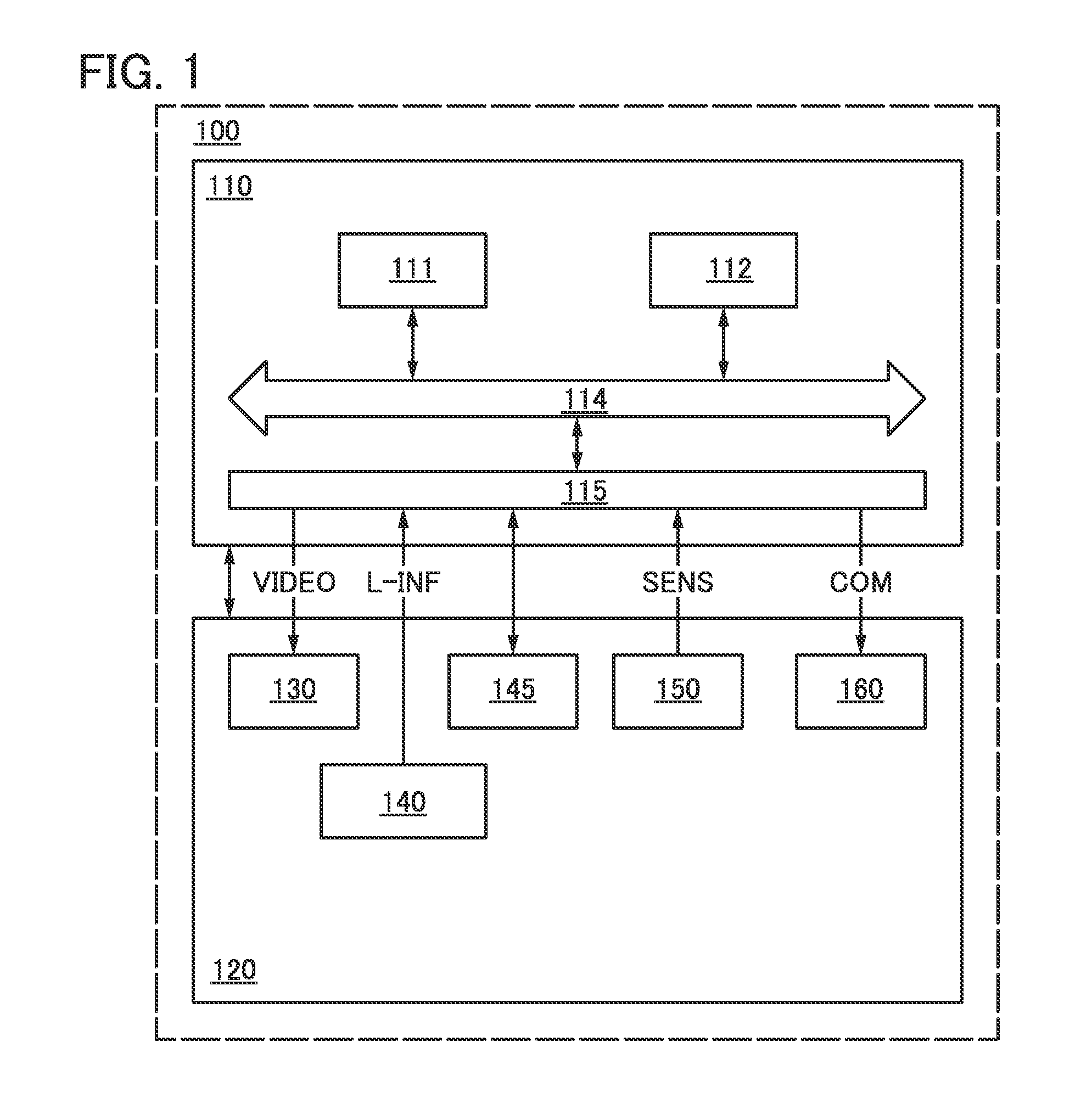
[0053]FIG. 1 shows a block diagram of a structure of a data processing device 100 of one embodiment of the present invention.
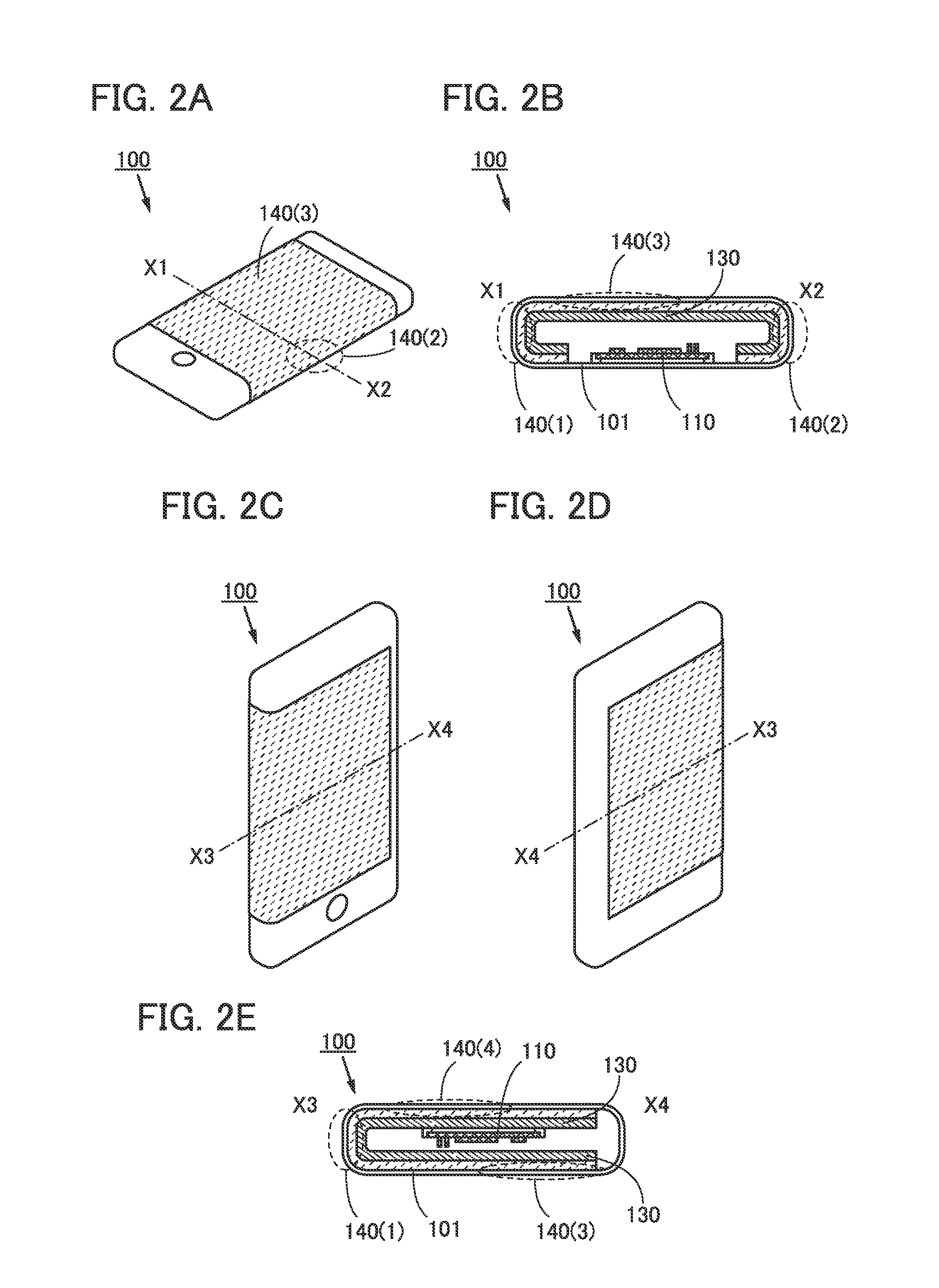
[0054]FIG. 2A is a schematic view illustrating the external appearance of the data processing device 100 of one embodiment of the present invention, and FIG. 2B is a cross-sectional view illustrating a cross-sectional structure along a cutting-plane line X1-X2 in FIG. 2A. FIGS. 2C and 2D are schematic views illustrating the external appearance of the data processing device 100 of one embodiment of the present invention, and FIG. 2E is a cross-sectional view illustrating a cross-sectional structure along a cutting-plane line X3-X4 in FIGS. 2C and 2D. FIG. 2C is a schematic view illustrating a front surface of the data processing device 100. FIG. 2D is a schematic view illustrating a back surface of the data pr...
embodiment 2
[0113]In this embodiment, the structure of the data processing device of one embodiment of the present invention will be described with reference to drawings.
[0114]FIG. 11 shows a block diagram of a structure of a data processing device 100B of one embodiment of the present invention.
[0115]FIGS. 12A to 12C are schematic views illustrating the external appearance of the data processing device 100B. FIG. 12A is the schematic view illustrating the external appearance of the data processing device 100B in an unfolded state, FIG. 12B is the schematic view illustrating the external appearance of the data processing device 100B in a bent state, and FIG. 12C is the schematic view illustrating the external appearance of the data processing device 100B in a folded state.
[0116]FIGS. 13A to 13E are schematic views illustrating the structures of the data processing device 100B. FIGS. 13A to 13D illustrate the structure in an unfolded state and FIG. 13E illustrates the structure in a folded state...
embodiment 3
[0163]In this embodiment, a structure of a data processing device of one embodiment of the present invention will be described with reference to drawings.
[0164]FIGS. 14A1, 14A2, 14B1, and 14B2 illustrate a state where the data processing device 100 of one embodiment of the present invention is held by a user. FIG. 14A1 illustrates the external appearance of the data processing device 100 held by a user, and FIG. 14A2 illustrates the ranges of a palm and fingers holding the data processing device 100 that are sensed by the proximity sensor in the position input portion 140 illustrated in FIG. 14A1. Note that the case where separate position input portions 140(A), 140(B), and 140(C) are used is illustrated in FIG. 17A. The description for the case of FIG. 17A can apply to the case of FIG. 14A2.
[0165]FIG. 14B1 is a schematic view where solid lines denote results of edge sensing processing of first positional data L-INF(1) sensed by the first region 140(1) of the position input portion ...
PUM
 Abstract
Description
Claims
Application Information
 - R&D
- Intellectual Property
- Life Sciences
- Materials
- Tech Scout
- Unparalleled Data Quality
- Higher Quality Content
- 60% Fewer Hallucinations
Browse by: Latest US Patents, China's latest patents, Technical Efficacy Thesaurus, Application Domain, Technology Topic, Popular Technical Reports.
© 2025 PatSnap. All rights reserved.Legal|Privacy policy|Modern Slavery Act Transparency Statement|Sitemap|About US| Contact US: help@patsnap.com


