
Sloped structure, method for manufacturing sloped structure, and spectrum sensor

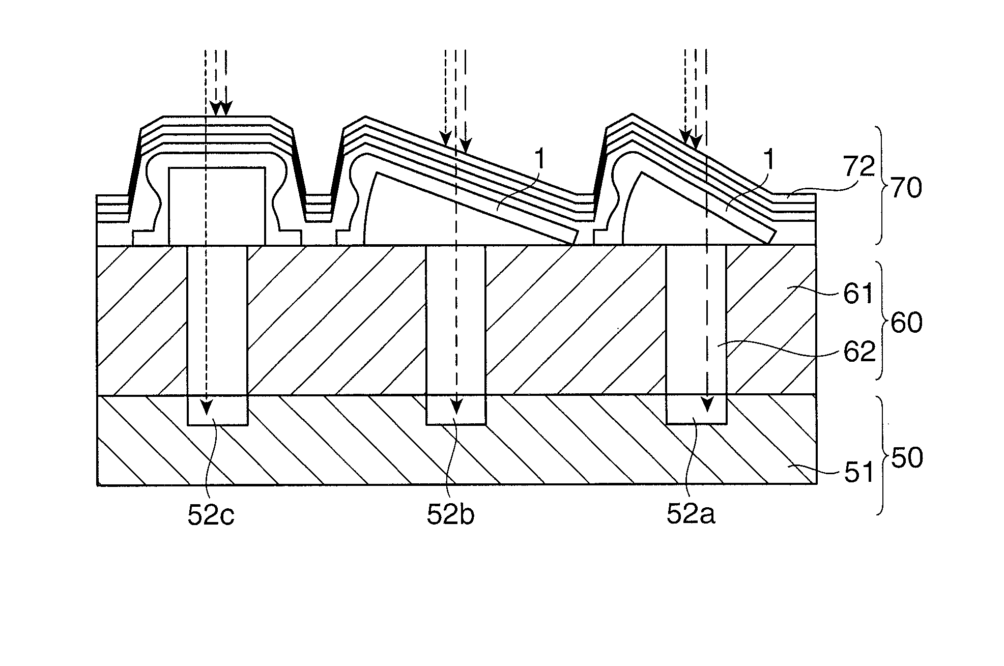
a technology of sloped structure and sloped structure, which is applied in the field of micro sloped structure, sloped structure manufacturing method, and spectrum sensor, can solve the problems of difficult manufacturing such micro structures and difficulty in size-reducing such spectrum sensors by the related art, and achieve the effect of improving the degree of freedom in selecting materials for the first film

Inactive Publication Date: 2014-10-09
SEIKO EPSON CORP
View PDF2 Cites 2 Cited by
  • Summary
  • Abstract
  • Description
  • Claims
  • Application Information

AI Technical Summary

Benefits of technology

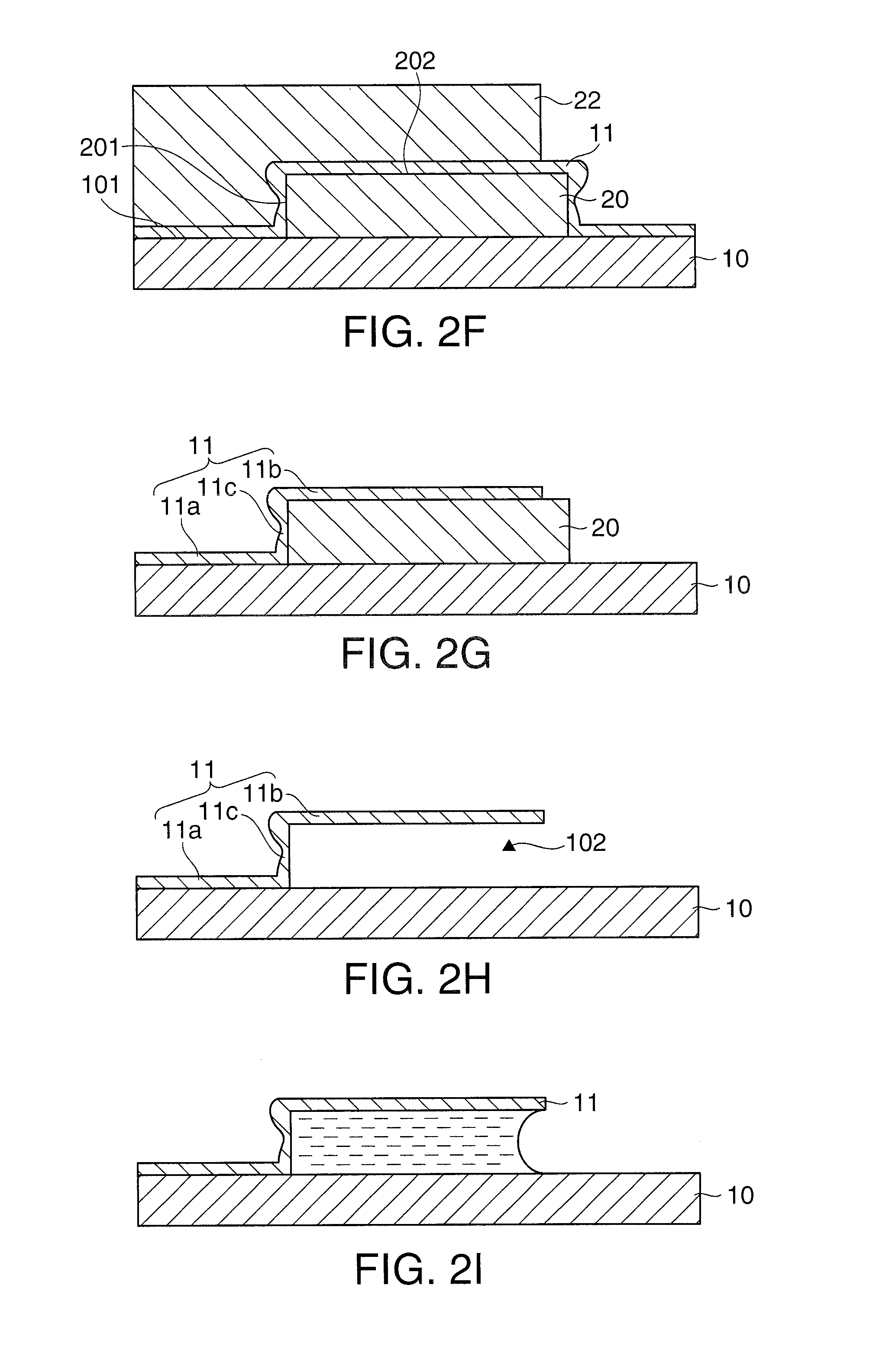
[0009]In accordance with an embodiment of the invention, a method for manufacturing a sloped structure includes the steps of; (a) forming a sacrificial film above a substrate; (b) forming a first film above the sacrificial film, the first film having a first portion connected to the substrate, a second portion located above the sacrificial film, a third portion located between the first portion and the second portion, and a thin region in a portion of the third portion or in a boundary section between the second portion and the third portion and having a thickness smaller than the first portion; (c) removing the sacrificial film; and, after the step (c), (d) bending the first film in the thin region thereby sloping the second portion of the first film with respect to the substrate. According to the aspect described above, a micro sloped structure can be readily manufactured with a process having high affinity to a semiconductor device fabrication process.
[0012]In the embodiment described above, the sacrificial film formed by the step (a) may preferably include a first layer and a second layer located above the first layer, and the step (e) may preferably include exposing the side surface of the sacrificial film by using etching liquid or etching gas that causes an etching rate of the first layer greater than an etching rate of the second layer. According to this aspect, the overhang and the thin section can be more readily formed.
[0014]In the embodiment described above, the step (d) may preferably include supplying liquid between the first film and the substrate, and then removing the liquid. According to this aspect, the first film can be bent and the second portion of the first film can be sloped with respect to the substrate, without having to apply an excessive force to the first film.

Problems solved by technology

However, size-reduction of such a spectrum sensor by the related art is difficult.
However, it has been difficult to manufacture such micro structures according to the related art.

Method used


Image

  • Sloped structure, method for manufacturing sloped structure, and spectrum sensor
  • Sloped structure, method for manufacturing sloped structure, and spectrum sensor
  • Sloped structure, method for manufacturing sloped structure, and spectrum sensor

Examples


first embodiment

1. First Embodiment

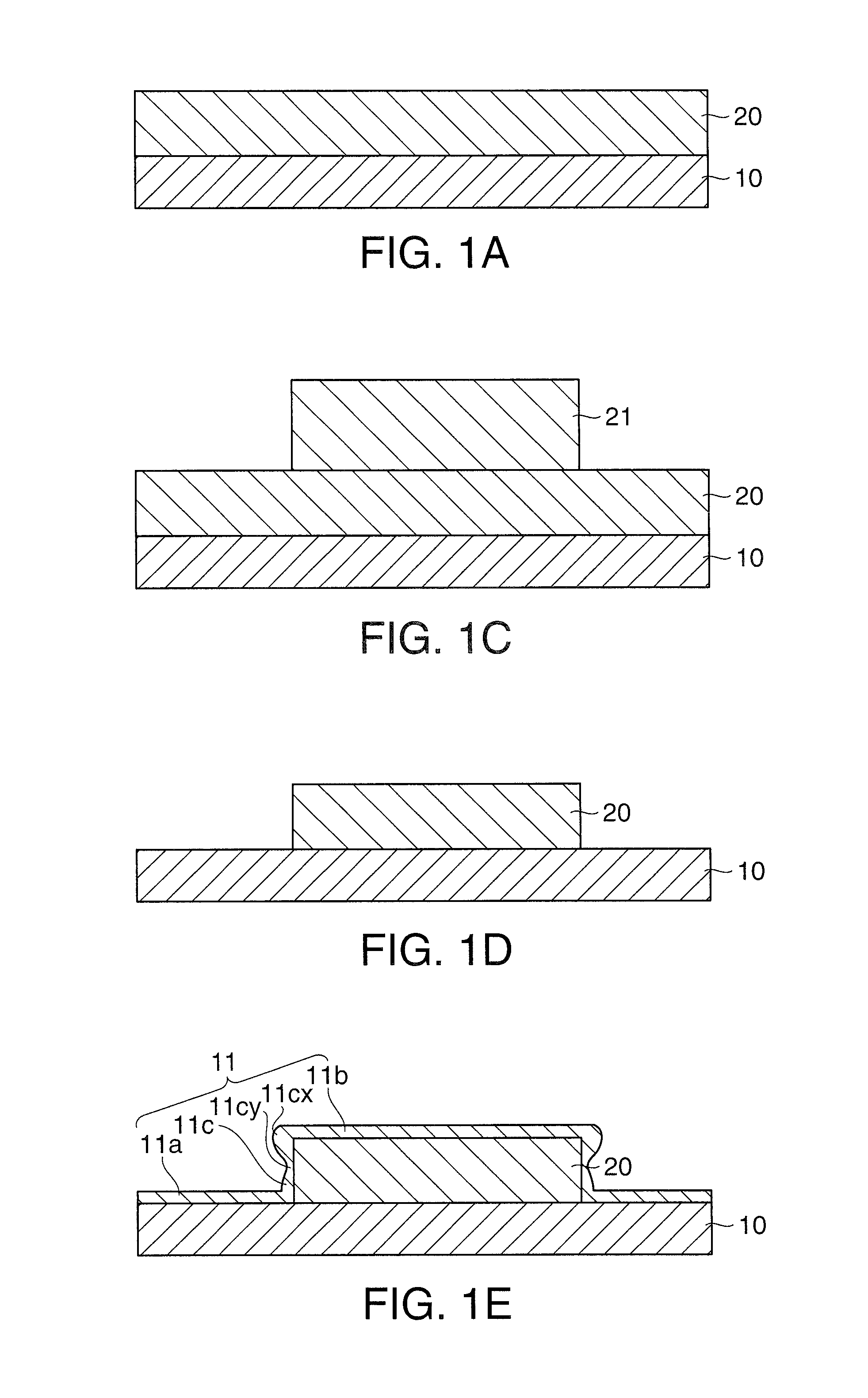
[0033]FIGS. 1-3 are cross-sectional views showing a method for manufacturing a sloped structure in accordance with a first embodiment of the invention. The manufacturing method in accordance with the present embodiment uses the semiconductor processing technology, thereby providing a low-cost manufacturing method that can readily achieve device miniaturization.

1-1. Film Formation of First Film

[0034]First, as shown in FIG. 1A, a sacrificial film 20 is formed on a substrate 10. The substrate 10 may be, for example, a silicon oxide (SiO2) substrate, or a silicon oxide substrate with an angle restriction filter (to be described below) formed thereon. As the sacrificial film 20, for example, a silicon nitride (SiN) film may be used.

[0035]Next, as shown in FIG. 1C, a resist film 21 is formed on the sacrificial film 20, and the resist film 21 is patterned into a predetermined shape (for example, a rectangular shape), by exposure and development of the resist film 21. The...

second embodiment

2. Second Embodiment

[0053]FIGS. 4-6 are cross-sectional views showing a method for manufacturing a sloped structure in accordance with a second embodiment of the invention. The manufacturing method in accordance with the second embodiment pertains to a method by which the overhang in the first film 11 can be more readily formed.

[0054]Steps shown in FIGS. 4-6 are generally the same in many aspects as those shown in FIGS. 1-3. However, they are different from the process shown in FIGS. 1-3 in that a sacrificial film 20 includes a first layer 20a and a second layer 20b.

[0055]First, as shown in FIG. 4A, a first layer 20a composing a sacrificial film 20 is formed on a substrate 10 that may be formed from, for example, silicon oxide or the like. Then, as shown in FIG. 4B, a second layer 20b composing the sacrificial film 20 is formed on the first layer 20a. The first layer 20a and the second layer 20b are formed from mutually different materials. For example, the first layer 20a may be f...

third embodiment

3. Third Embodiment

[0061]FIGS. 7-8 are cross-sectional views showing in part a method for manufacturing a sloped structure in accordance with a third embodiment of the invention. The manufacturing method in accordance with the third embodiment pertains to a method by which the overhang in the first film 11 can be more readily formed.

[0062]Steps shown in FIGS. 7 and 8 are generally the same in many aspects as those shown in FIGS. 4 and 5. However, as shown in FIG. 7A and FIG. 7B, the process in accordance with the third embodiment is different from the process shown in FIGS. 4 and 5 in that a second layer 20c of a sacrificial film 20 is formed by surface property modification of the sacrificial film 20.

[0063]First, as shown in FIG. 7A, a sacrificial film 20 of silicon (Si) or the like is formed on a substrate 10 of silicon oxide or the like. Then, as shown in FIG. 7B, ions are injected in the sacrificial film 20, thereby conducting surface property modification of the sacrificial fil...


PUM


Abstract

A method for manufacturing a sloped structure is disclosed. The method includes the steps of: (a) forming a sacrificial film above a substrate; (b) forming a first film above the sacrificial film, the first film having a first portion connected to the substrate, a second portion located above the sacrificial film, a third portion located between the first portion and the second portion, and a thin region in a portion of the third portion or in a boundary section between the second portion and the third portion and having a thickness smaller than the first portion; (c) removing the sacrificial film; and (d) bending the first film in the thin region, after the step (c), thereby sloping the second portion of the first film with respect to the substrate.

Description

[0001]This is a Division of application Ser. No. 13 / 572,192 filed Aug. 10, 2012, which claims priority to Japanese Patent Application No. 2011-179646, filed Aug. 19, 2011. The disclosures of the prior applications are hereby incorporated by reference herein in their entirety.BACKGROUND[0002]1. Technical Field[0003]The present invention generally relates to micro sloped structures, methods for manufacturing a sloped structure, and spectrum sensors using the sloped structure.[0004]2. Related Art[0005]Spectrum sensors are used in the medical, agricultural and environmental fields for diagnosing and examining objects. For example, in the medical field, a pulse oximeter is used to measure the oxygen saturation of blood, using light absorption of hemoglobin. Also, in the agricultural field, a saccharometer is used to measure the concentration of sugar content of fruits, using light absorption of sugar.[0006]Japanese Laid-open Patent Application HEI 6-129908 (related art) describes a spect...

Claims


Application Information

Patent Timeline
Patent Type & Authority Applications(United States)
IPC IPC(8): H01L31/0236H01L31/18
CPCH01L29/06G02B5/201G02B5/285G01J3/0256G01J3/36G01J2003/1213H01L31/18B81B2201/047B81B2203/0384H01L31/02165H01L31/02327H01L31/02366G01J1/0488
Inventor YOSHIZAWA, TAKAHIKO
Owner SEIKO EPSON CORP
Learn More