Array substrate and driving method thereof and display device

a technology which is applied in the field of array substrate and driving method thereof, can solve the problems of h-line badness, influence on the yield of products, and the difference of displaying between rows in the displaying process so as to avoid h-line badness of the display device, reduce the resistance difference between the gate lines in two adjacent rows, and reduce the quantity of wiring of the gate lines

Inactive Publication Date: 2014-07-31
BEIJING BOE OPTOELECTRONCIS TECH CO LTD
View PDF3 Cites 1 Cited by
  • Summary
  • Abstract
  • Description
  • Claims
  • Application Information

AI Technical Summary

Benefits of technology

[0015]In the array substrate and the driving method thereof and the display device provided in the embodiments of the present invention, one gate line controls the first pixel unit and the second pixel unit in two adjacent rows which are adjacent to the gate line, the first pixel unit is charged by using the first data line, the second pixel unit is charged by using the second data line, and signals are sequentially output to the first pixel unit and the second pixel unit through the first data line and the second data line to realize progressive scanning of the array substrate, wherein, the two adjacent gate lines on the periphery of the pixel units are formed by metal of the same layer. In this way, the quantity of wiring of the gate lines may be effectively reduced, and the wiring of the gate lines with single-layer metal is realized; and since the gate lines may be formed by adopting the same mask process, the resistance difference between the gate lines in two adjacent rows is reduced, H-line badness of the display device is avoided, and the yield of the display device product is improved.

Problems solved by technology

The array substrate with such structure has following shortcomings: lines on the periphery of the pixel units 13 are generally long, large resistance difference is produced between metal of different layers, and particularly for the thin gate lines, the resistance difference between gate lines in two adjacent rows is overally high, which readily results in a difference of displaying between the rows in the displaying process of the display device and causes H-line badness.
Such shortcomings have adverse influence on the yield of the product.

Method used


Image

  • Array substrate and driving method thereof and display device
  • Array substrate and driving method thereof and display device
  • Array substrate and driving method thereof and display device

Examples


Embodiment Construction

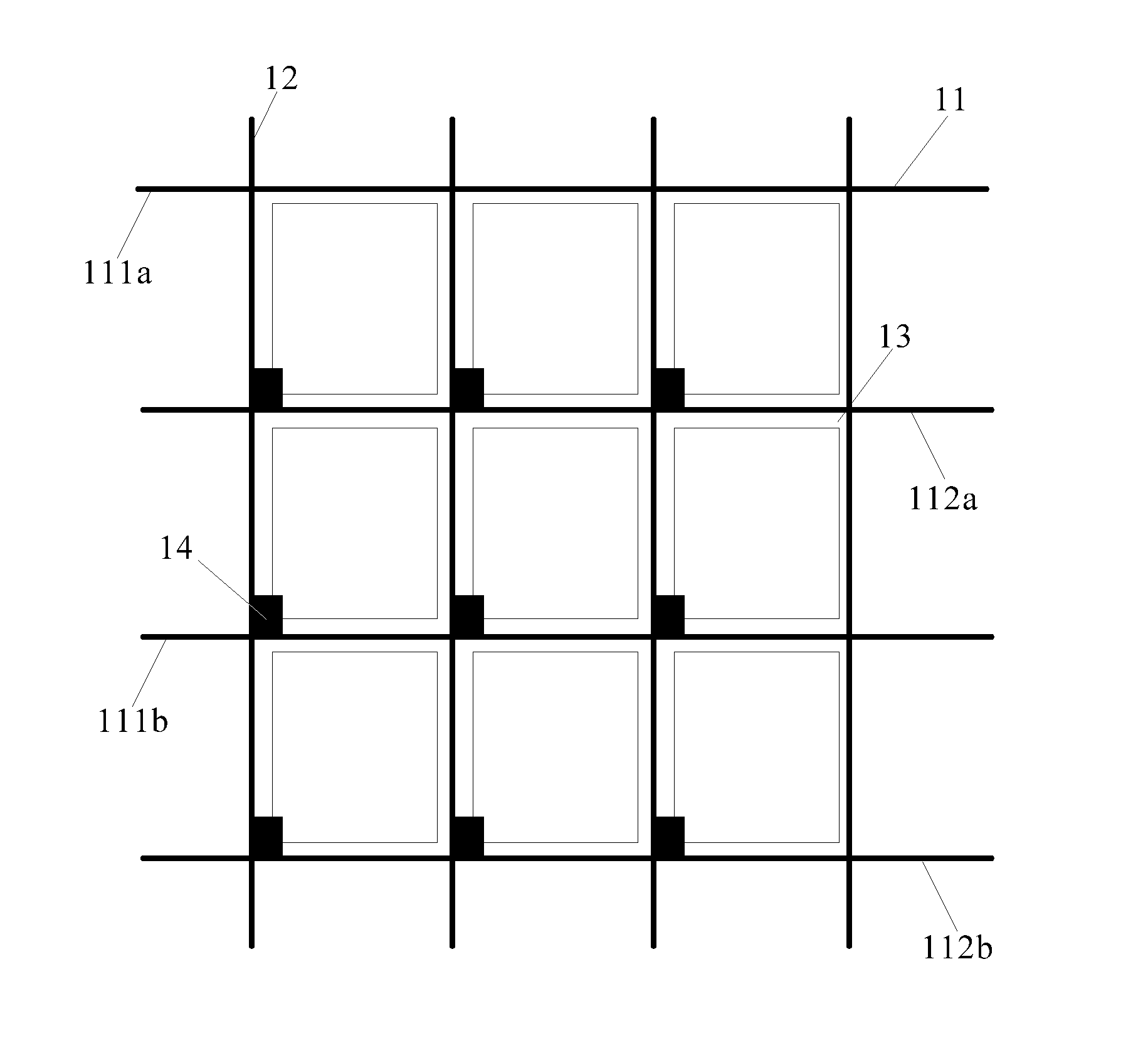
[0024]A clear and complete description of technical solutions in the embodiments of the present invention will be given below, in combination with the accompanying drawings in the embodiments of the present invention. Apparently, the embodiments described herein are merely a part, but not all, of the embodiments of the present invention. All of other embodiments, obtained by those of ordinary skill in the art based on the embodiments in the present invention, fall into the protection scope of the present invention.

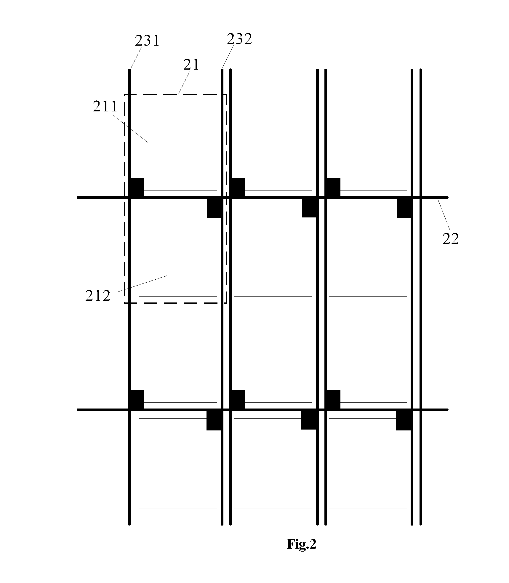
[0025]An array substrate provided in an embodiment of the present invention, as shown in FIG. 2, includes: multiple pixel groups 21 arranged in a matrix form, multiple rows of gate lines 22 corresponding to the respective pixel groups 21 and arranged transversely, and multiple columns of first data lines 231 and multiple columns of second data lines 232 arranged longitudinally.

[0026]Each pixel group 21 includes a first pixel unit 211 and a second pixel unit 212, which are ...


PUM


Abstract

Embodiments of the present invention provide an array substrate and a driving method thereof and a display device. The array substrate includes multiple pixel groups arranged in a matrix form, multiple rows of gate lines arranged transversely which are corresponding to the pixel groups, and multiple columns of first and second data lines arranged longitudinally, wherein each pixel group includes a first pixel unit and a second pixel unit which are located in two adjacent rows; the gate line is connected to the first and second pixel unit in the corresponding pixel group respectively, the first and second data lines are respectively connected with the first and second pixel units in the corresponding pixel group to provide data signals to the first and second pixel units; wherein, the gate lines on the periphery of the pixel units are formed by metal of the same layer.

Description

FIELD OF THE INVENTION[0001]The present invention relates to the field of display technology, in particular to an array substrate and a driving method thereof and a display device.BACKGROUND OF THE INVENTION[0002]At present, a display device with narrow frame has gradually become the mainstream development of display products, and the key to obtain a display device with a narrower frame is to reduce an area occupied by a gate line or data line circuit around a display area in an array substrate.[0003]An existing array substrate may be as shown in FIG. 1, including multiple pixel units 13 segmented by gate lines 11 and data lines 12 crossed transversely and longitudinally, wherein the inside of each pixel unit 13 has a TFT (Thin Film Transistor) area 14, and the gate lines 11 and the data lines 12 drive the pixel units 13 to work through the TFTs in the TFT areas 14. In the existing array substrate, all the gate lines within the area of the pixel units 13 may be formed by metal of th...

Claims


Application Information

Patent Timeline
Patent Type & Authority Applications(United States)
IPC IPC(8): G09G3/36H01L27/12
CPCG09G3/3659H01L27/124G09G3/20G09G3/2085G09G3/3648G09G2300/0426G09G2320/0223G09G2300/0465G09G2310/0218
Inventor LI, YUEXUE, YANNAWANG, LEI
Owner BEIJING BOE OPTOELECTRONCIS TECH CO LTD
Why Eureka
Try Eureka