Touch sensing panel
a touch sensor and panel technology, applied in the field of touch sensing panels, can solve the problems of increasing user dissatisfaction and the inability to obtain an exact touch position, and achieve the effect of improving touch input performance and improving touch precision
- Summary
- Abstract
- Description
- Claims
- Application Information
AI Technical Summary
Benefits of technology
Problems solved by technology
Method used
Image
Examples
first embodiment
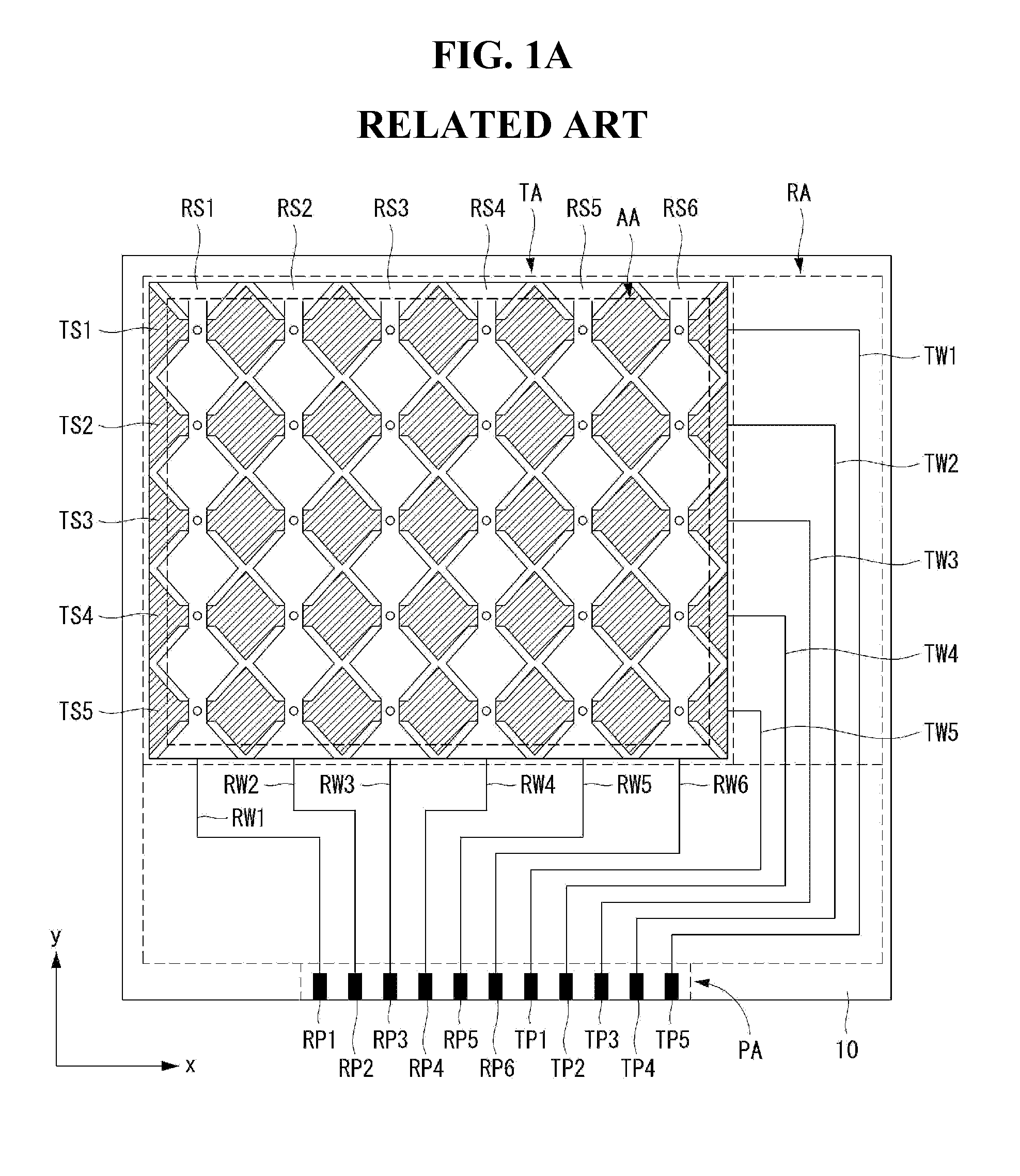
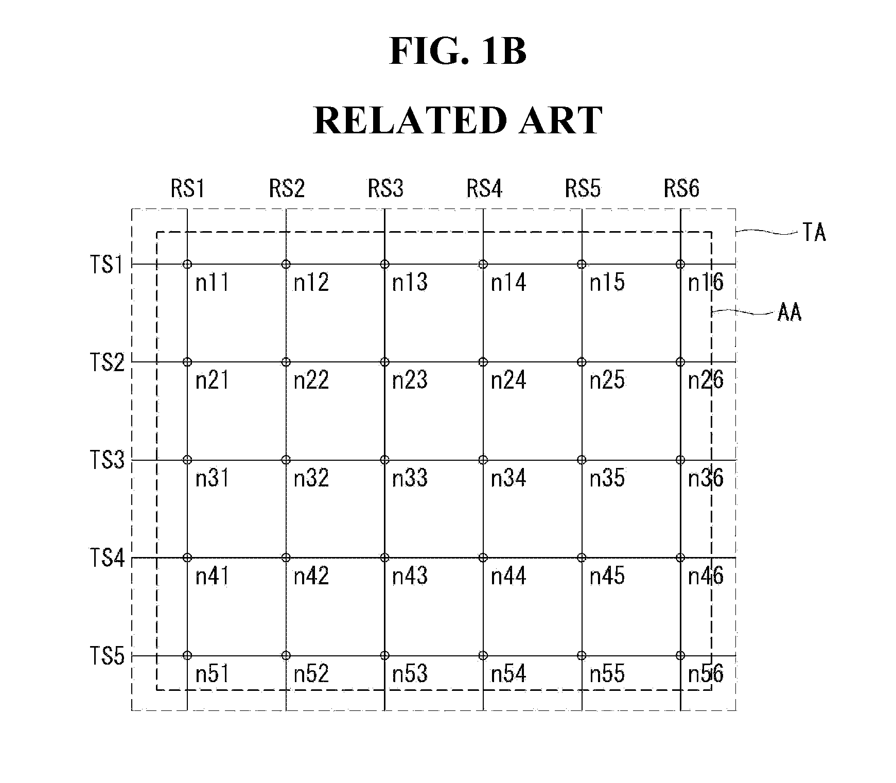
[0046]Referring to FIGS. 3A, 3B and 4, the touch sensing panel according to this disclosure includes a touch electrode formation area TA, an active area AA, a routing wiring formation area RA, and a pad formation area PA. Touch electrodes, provided with touch drive electrodes and touch sensing electrodes, are formed on the touch electrode formation area TA. The active area AA corresponds to a display area of a display apparatus (not illustrated) on which display data are displayed. Routing wirings, connected to the touch electrodes formed on the touch electrode formation area TA, are formed on the routing wiring formation area RA. Routing pads for connecting the routing wirings and signal lines of a touch drive circuit (not illustrated) are formed on the pad formation area PA.
[0047]The touch electrode formation area TA includes a plurality of first touch electrode serials TS1 to TS5 (touch drive electrode serials or touch sensing electrode serials), a plurality of second touch elect...
second embodiment
[0058]The sensing nodes are formed in the touch electrode formation area TA outside of the active area AA. In the touch sensing panel according to this disclosure, the sensing nodes n11, n12, n13, n14, n15, and n16 are formed in the touch electrode formation area TA1 outside of the uppermost edge of the active area AA. And the sensing nodes n51, n52, n53, n54, n55, and n56 are formed in the touch electrode formation area TA2 outside of the lowermost edge of the active area AA. And the sensing nodes n11, n21, n31, n41, and n51 are formed in the touch electrode formation area TA3 outside of the leftmost edge of the active area AA. And the sensing nodes n16, n26, n36, n46, and n56 are formed in the touch electrode formation area TA4 outside of the rightmost edge of the active area AA.
[0059]Reference character CL denotes a cutting line in the touch sensing panel according to the second embodiment shown in FIG. 5. However, the cutting line CL is formed in such a manner that the outermost...
third embodiment
[0066]Referring to FIGS. 7A, 7B, 8A and 8B, the touch sensing panel according to this disclosure includes a touch electrode formation area TA, an active area AA, a routing wiring formation area RA, and a pad formation area PA. Touch electrodes are formed on the touch electrode formation area TA. The active area AA corresponds to a display area of a display apparatus (not illustrated) on which display data are displayed. Routing wirings are formed on the routing wiring formation area RA, in order to transmit and receive a signal to and from the touch electrode formation area TA. Routing pads for connecting the routing wirings and signal lines of a touch drive circuit (not illustrated) are formed on the pad formation area PA.
[0067]The touch sensing panel according to the third embodiment is different from the touch sensing panel according to the first embodiment in that electrode patterns of the first touch electrode serials that are on a borderline of the active area AA or are adjace...
PUM
 Abstract
Description
Claims
Application Information
 - R&D
- Intellectual Property
- Life Sciences
- Materials
- Tech Scout
- Unparalleled Data Quality
- Higher Quality Content
- 60% Fewer Hallucinations
Browse by: Latest US Patents, China's latest patents, Technical Efficacy Thesaurus, Application Domain, Technology Topic, Popular Technical Reports.
© 2025 PatSnap. All rights reserved.Legal|Privacy policy|Modern Slavery Act Transparency Statement|Sitemap|About US| Contact US: help@patsnap.com


