
Method for detecting and debugging design errors in low power IC design

a low-power ic design and error detection technology, applied in the field of low-power ic design error detection and debugging, can solve the problems of cumbersome detection and debugging of ic designers, difficult for designers to have a full picture in mind for detecting and debugging anomalies or errors between ic design and power specification, and the complexity of system-on-chip (soc) design becomes much more complex and difficult to debug

Active Publication Date: 2013-11-14
SYNOPSYS INC
View PDF1 Cites 39 Cited by
  • Summary
  • Abstract
  • Description
  • Claims
  • Application Information

AI Technical Summary

Benefits of technology

The present invention provides a way to detect and fix problems in a low power IC design. This includes checking the power design and the interactions between them. The invention identifies problem areas in the circuit design and power specification, and provides information on the root cause of the problem. This makes it easier for designers to fix issues early on in the design process. The invention also includes a debugger that helps designers analyze and fix issues with the circuit design. Overall, this invention streamlines the process of developing low power IC designs and improves their quality.

Problems solved by technology

For example, system-on-chip (SoC) design becomes much more complex and harder to debug as more and more digital circuit and low power network designs are integrated into one chip.
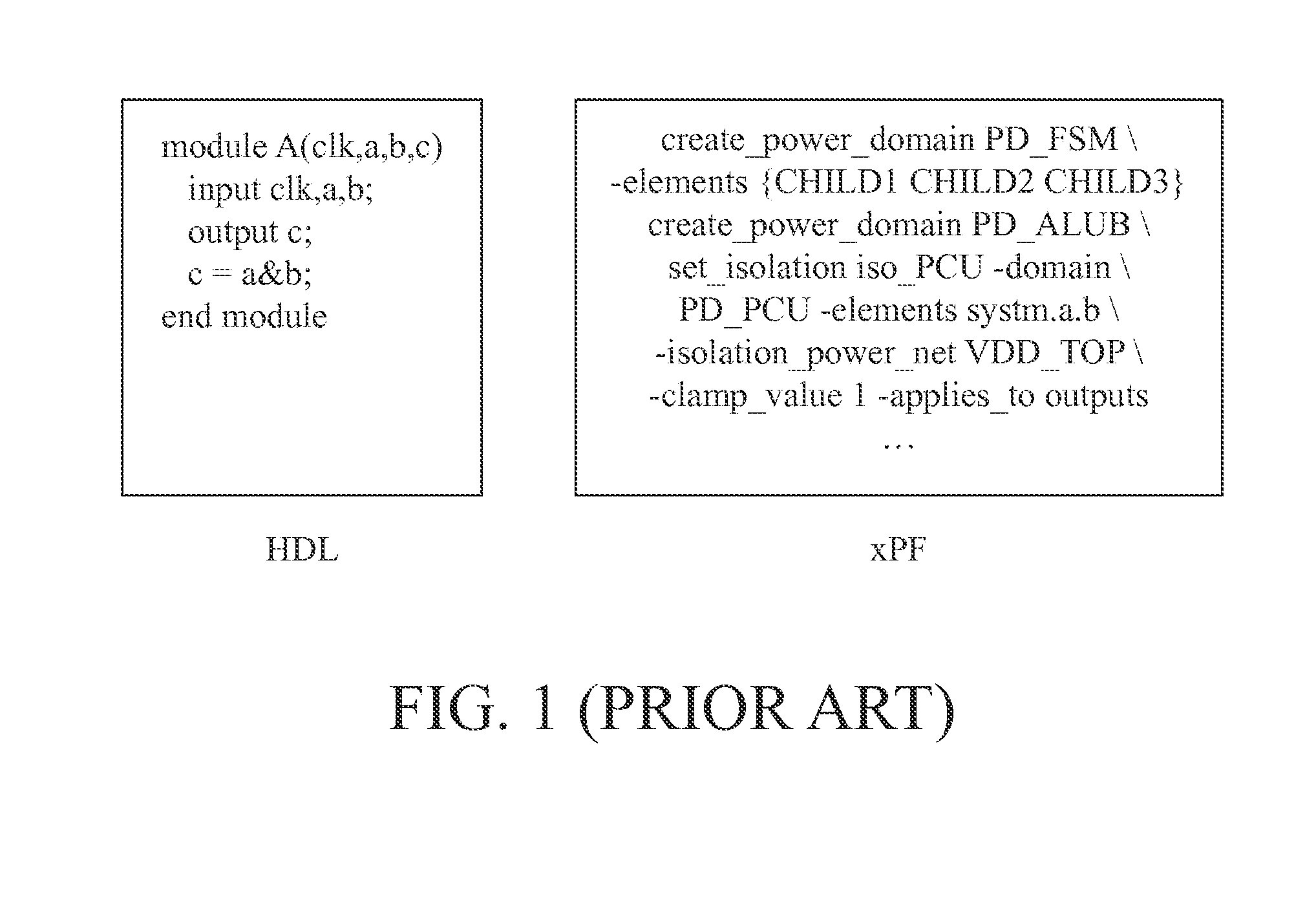
Since traditional hardware description languages (HDL) are not adequate to specify the power design information, power formats, such as xPF files, provide a format without touching the existing HDL codes.
Because HDL descriptions and xPF descriptions are in separate files, it is cumbersome for IC designers to detect and debug when there is an anomaly in signal behaviors.
Moreover, both HDL and xPF are text descriptions, which make it even harder for designers to have a full picture in mind for detecting and debugging anomalies or errors between the IC design and power specification.

Method used


Image

  • Method for detecting and debugging design errors in low power IC design
  • Method for detecting and debugging design errors in low power IC design
  • Method for detecting and debugging design errors in low power IC design

Examples


Embodiment Construction

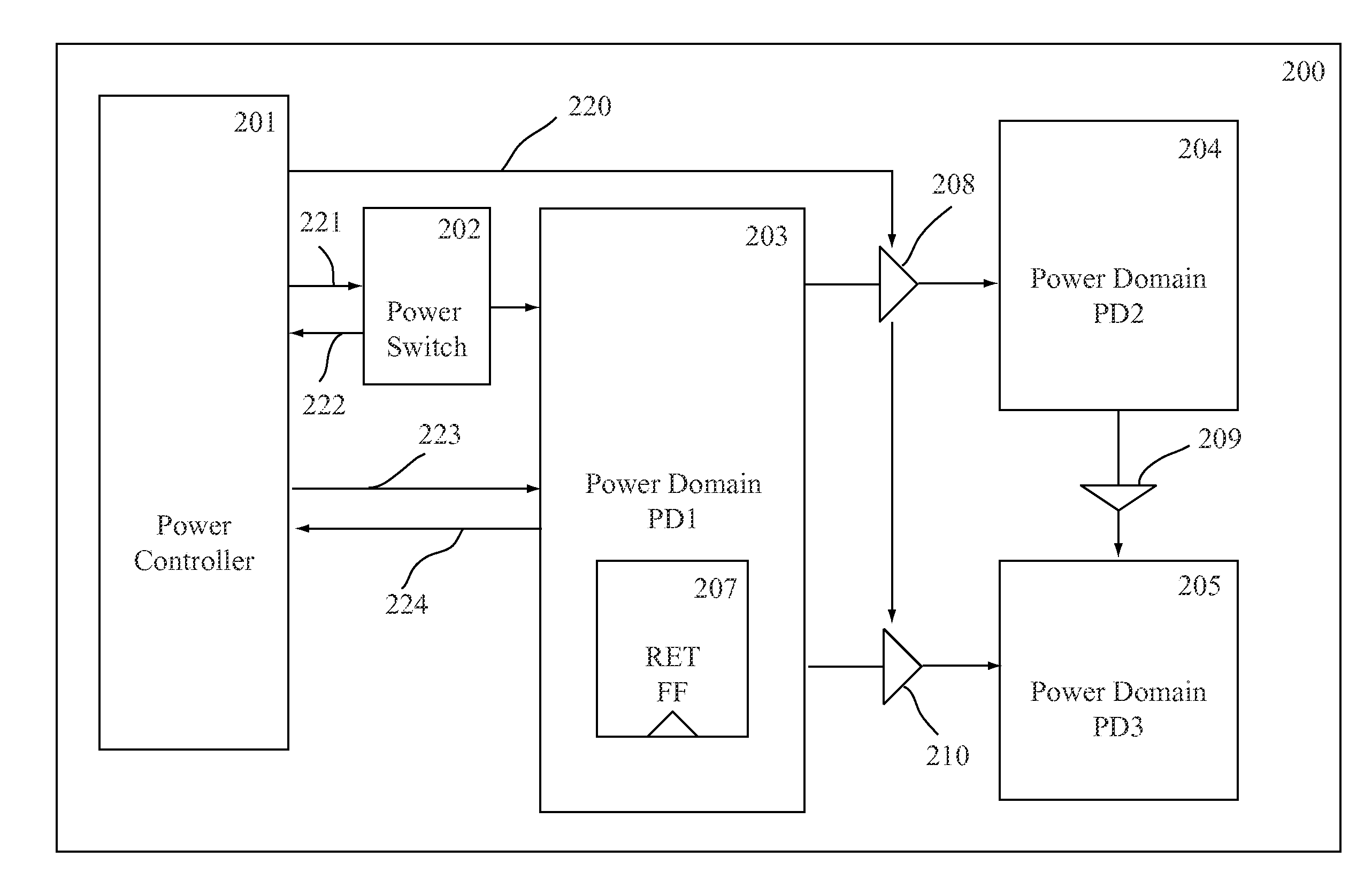
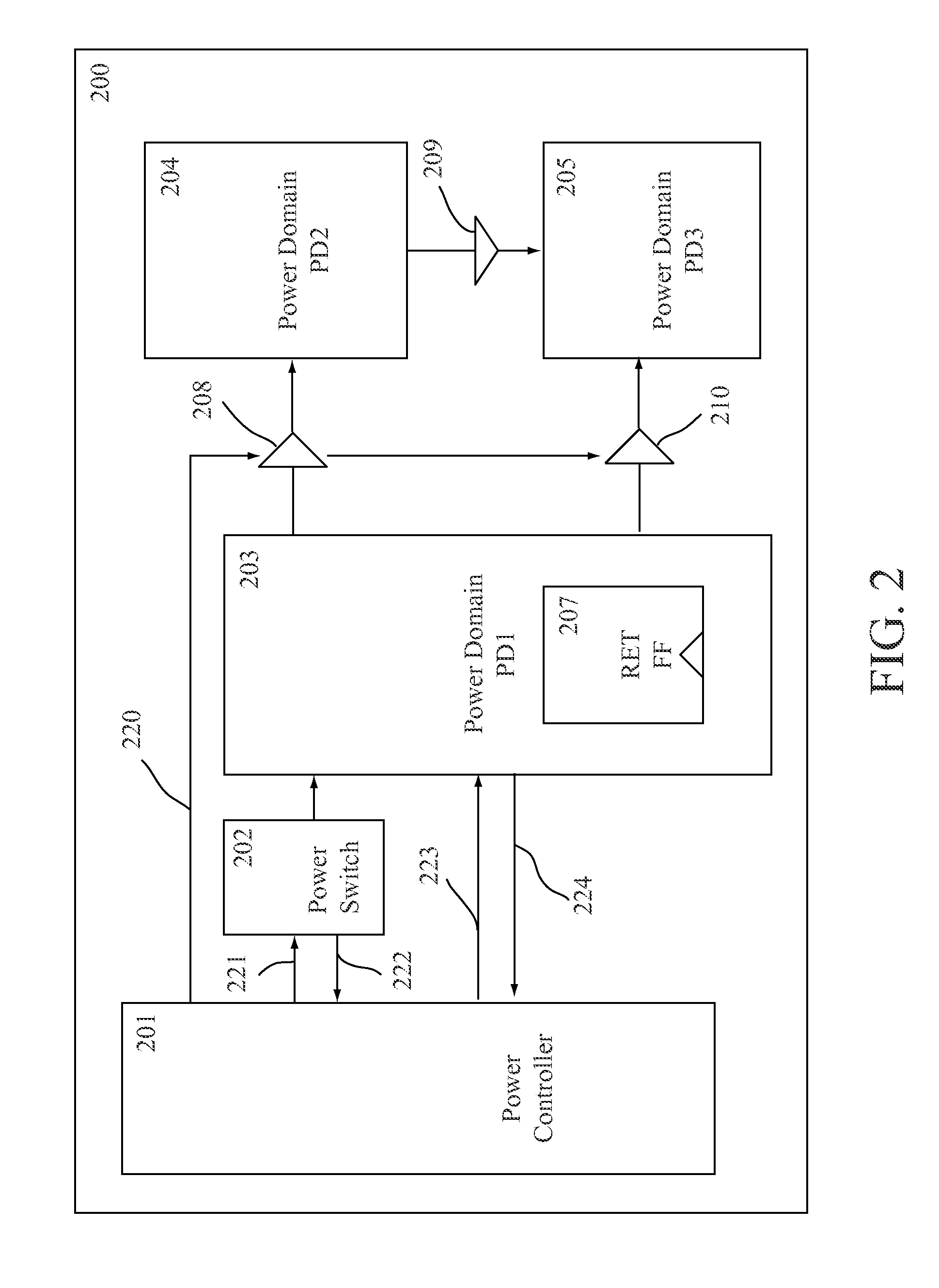
[0021]The embodiments are presented for purposes of illustrations only, they are not intended to limit the scope of the present invention. An IC design is typically performed using electronic design automation (EDA) tools running on a computing apparatus (computer, server). A designer captures an IC design using schematic editor or describes the IC design using a high-level description language. A low power IC design is generally partitioned into many parts according to their functions and speed requirements. A netlist can be created to define the parts and specifies how the parts are interconnected. The netlist can be used for simulation and implementation of the design. A power specification can be generated to insert specific cells or blocks to guide the implementation of the low power IC design. The power specification is generated in a file separate from the IC design file. The following sections will describe a method for detecting and debugging anomalies or errors in the desi...


PUM


Abstract

A method for detecting anomalies in signal behaviors in a simulation of a low power IC includes receiving a circuit design and a power specification of the IC, determining at least one power sequence checking rule from the power specification, simulating the circuit design and the power specification to obtain a dump file, identifying at least one anomaly of the at least one power sequence checking rule based on the dump file, and generating information relevant to the identified anomaly of the at least one power sequence checking rule. The method further includes setting up a context in a debugger for debugging the anomaly by displaying a waveform of misbehaved signals associated with the anomaly in a waveform window, and a portion of the circuit design and / or a portion of the power specification associated with the anomaly in a text window.

Description

CROSS-REFERENCES TO RELATED APPLICATIONS[0001]This application claims the benefit of and priority to U.S. Provisional Application No. 61 / 645,071, filed May 10, 2012, the entirety of which is incorporated by reference herein for all purposes.BACKGROUND OF THE INVENTION[0002]1. Field of the Invention[0003]The present invention relates to debugging a low power IC design and, in particular, to debugging of a low power IC design using power sequence checking rules.[0004]2. Description of the Related Art[0005]With the rapid progress of mobile devices and consumer electronic equipment in recent years, there are more and more sophisticated gadgets that are available to the public, such as smart cellular phones, personal mobile computers, MP3 audio players, notebooks and digital cameras. As additional functions and low power consumption are needed in thinner and lighter electronic products, IC designers wish to integrate varieties of discrete components on one chip to suit these requirements...

Claims


Application Information

Patent Timeline
IPC IPC(8): G06F17/50
CPCG06F17/5009G06F30/367G06F2119/06G06F30/20
Inventor HSIEH, MING HANHSU, CHIH-NENGHSIEH, MING-HUI
Owner SYNOPSYS INC
Learn More