Manufacturing Method of Waveguide Having a Metal Alignment Mark

a waveguide and metal alignment technology, applied in the field of waveguide structure, can solve the problems of inability to obtain efficient systems, difficulty in coupling of light sources to waveguides, and limitation of magnetic recording in which only magnetic fields are utilized for recording data, so as to reduce beam loss and efficiently remove polarization

Active Publication Date: 2013-01-24
SEAGATE TECH LLC
View PDF3 Cites 2 Cited by
  • Summary
  • Abstract
  • Description
  • Claims
  • Application Information

AI Technical Summary

Benefits of technology

The present invention provides a waveguide structure with an efficient metal alignment mark to reduce beam-loss and remove polarization present in an undesirable direction. A proper lower clad thickness is maintained to minimize propagation loss from an absorbing material. These improvements allow for a better beam intensity and shape after passing through a nano-aperture. Additionally, a metal alignment mark is formed to efficiently remove transverse magnetic (TM) mode and to efficiently determine a location of a nano-aperture.

Problems solved by technology

As generally known in the art, the practice of magnetic recording in which only a magnetic field is utilized for recording data has a limitation in high-density recording due to thermal instability.
Also, if a profile of the 3D waveguide is similar to a slab for the purpose of attaining a high polarization dependent loss (PDL) as in a cavity of a laser diode, coupling of the light source to the waveguide becomes difficult and thus an efficient system can not be obtained.
Further, since the loss of the beam and the polarization in an undesirable direction occur when the beam is transmitted through the waveguide 35, there are the problems in that the beam intensity decreases and the shape of the beam changes after passing through the nano-aperture 37.

Method used


Image

  • Manufacturing Method of Waveguide Having a Metal Alignment Mark
  • Manufacturing Method of Waveguide Having a Metal Alignment Mark
  • Manufacturing Method of Waveguide Having a Metal Alignment Mark

Examples


Embodiment Construction

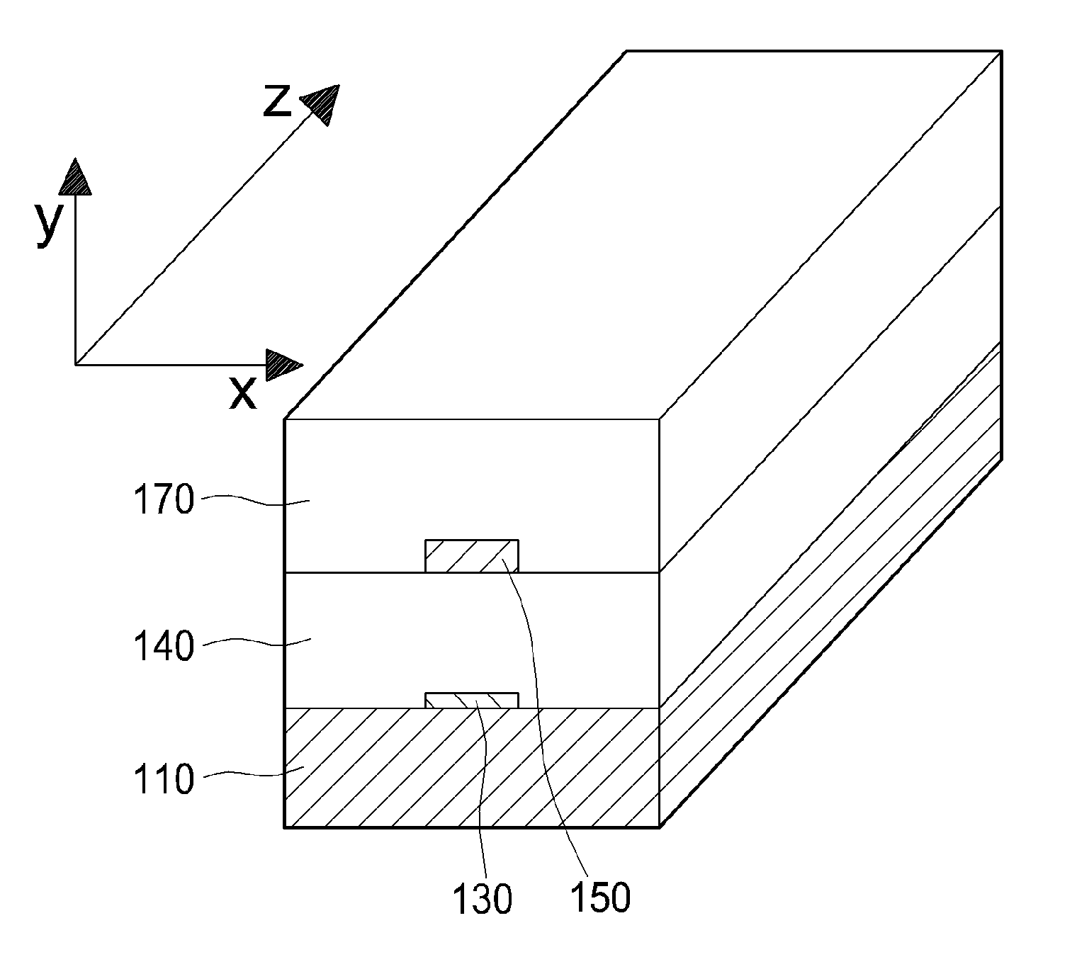
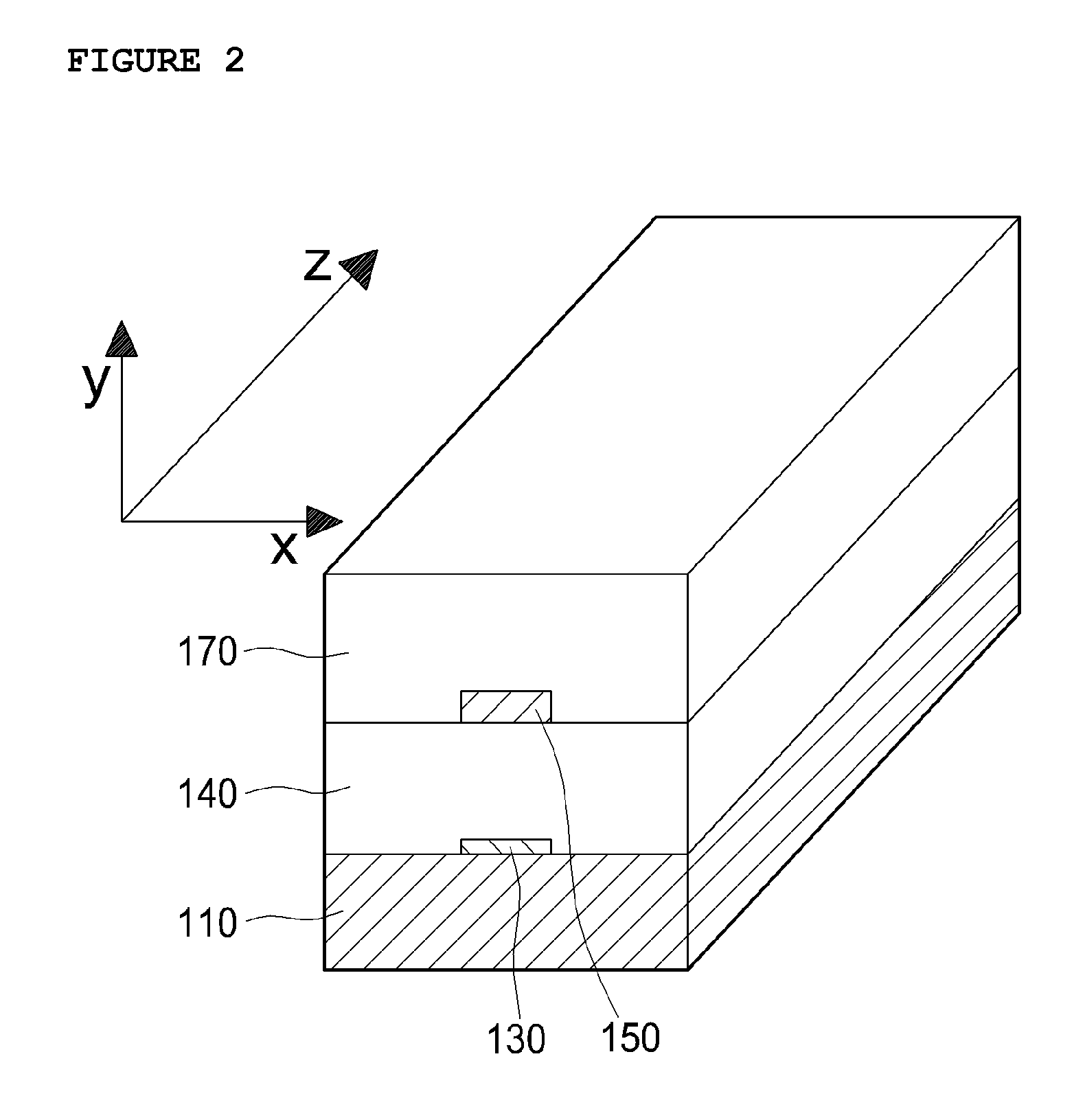
[0033]Hereinafter, a preferred exemplary embodiment of the present invention will be described with reference to the accompanying drawings. In the following description and drawings, the same reference numerals are used to designate the same or similar components, and so repetition of the description on the same or similar components will be omitted.

[0034]A waveguide structure, a manufacturing method thereof and a heat assisted magnetic recording head using the same are provided. A heat assisted portion comprises a waveguide and a nano-aperture formed at an end of the waveguide. An alignment mark is formed under a lower clad layer in order to make the waveguide and the nano-aperture an integrated type. Accordingly, there are advantages in that a location of an aperture to be formed may be readily determined, the propagation loss due to the presence of metal may be minimized by appropriately adjusting the thickness of the lower clad layer and it is possible to remove an undesired mod...


PUM

PropertyMeasurementUnit
wavelengthsaaaaaaaaaa
distanceaaaaaaaaaa

Abstract

A waveguide structure includes a metal layer of a predetermined size on a substrate, a lower clad layer on the structure completely covering the metal layer, a core layer of a predetermined size on the lower clad layer at the location corresponding to the metal layer, and an upper clad layer thereon completely covering the core layer.

Description

CROSS-REFERENCE TO RELATED PATENT APPLICATION[0001]This application is a divisional of U.S. patent application Ser. No. 11 / 972,207 filed on Jan. 10, 2008, to issue as U.S. Pat. No. 8,225,482 on Jul. 24, 2012, and claims the benefit of Korean Patent Application No. 10-2007-0003058, filed on Jan. 10, 2007, in the Korean Intellectual Property Office, both of which are incorporated herein by reference in their respective entireties.BACKGROUND OF THE INVENTION[0002]1. Field of the Invention[0003]The present invention relates to a waveguide structure, a manufacturing method thereof and a heat assisted magnetic recording head (HAMR) using the same, and more particularly to a waveguide structure, a manufacturing method thereof and a heat assisted magnetic recording head, wherein the improvement of beam intensity and the maintenance of a single focusing spot are attained even after an input beam passes through a nano-aperture.[0004]2. Description of the Prior Art[0005]As generally known in t...

Claims


Application Information

Patent Timeline
Patent Type & Authority Applications(United States)
IPC IPC(8): G02B6/10
CPCG02B6/122G11B5/314Y10T29/49002Y10T29/49016G11B2005/0021G02B6/10G11B5/127
Inventor SUH, SUNG-DONGCHO, EUN-HYOUNGSOHN, JIN-SEUNG
Owner SEAGATE TECH LLC
Why Eureka
Try Eureka