
Electrode structure for use in electronic device and method of making same

a technology of electronic devices and electrodes, applied in the direction of sustainable manufacturing/processing, semiconductor devices, climate sustainability, etc., can solve the problems of sodium (na) dispersing into the coating in an uncontrollable and predictable manner, undesirable and/or unpredictable functionality, etc., to prevent or reduce sodium (na) migration

Inactive Publication Date: 2013-01-24
GUARDIAN GLASS LLC
View PDF3 Cites 7 Cited by
  • Summary
  • Abstract
  • Description
  • Claims
  • Application Information

AI Technical Summary

Benefits of technology

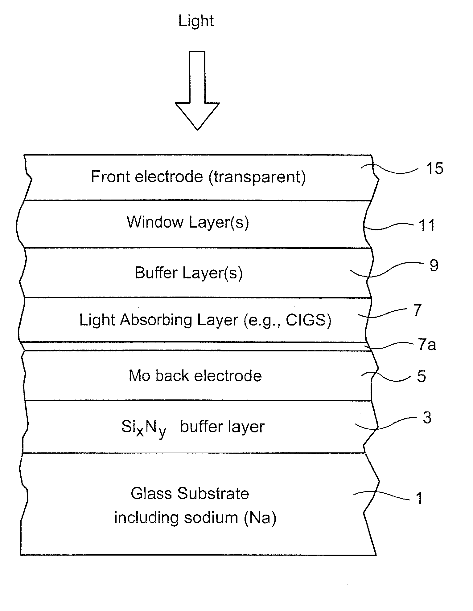
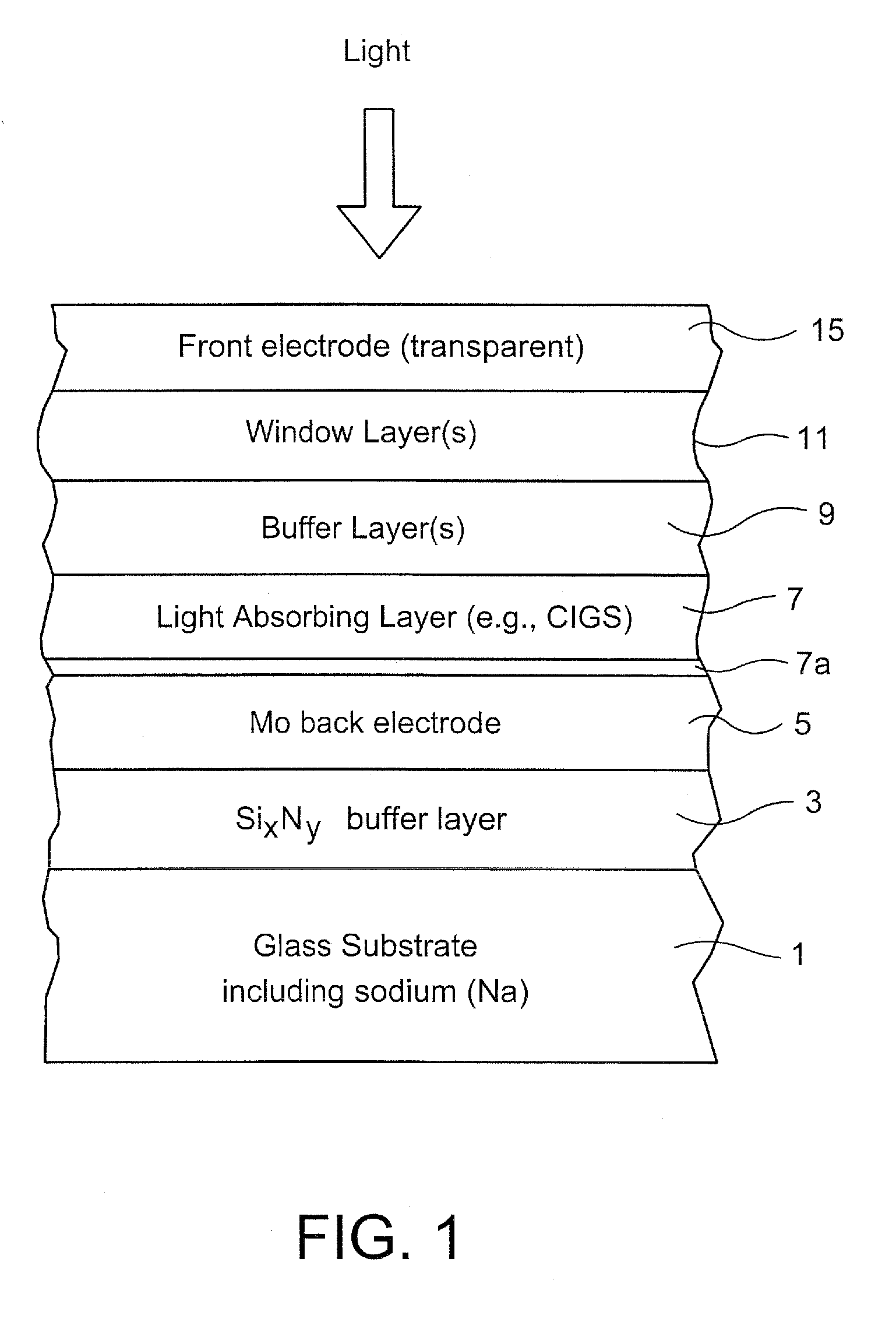
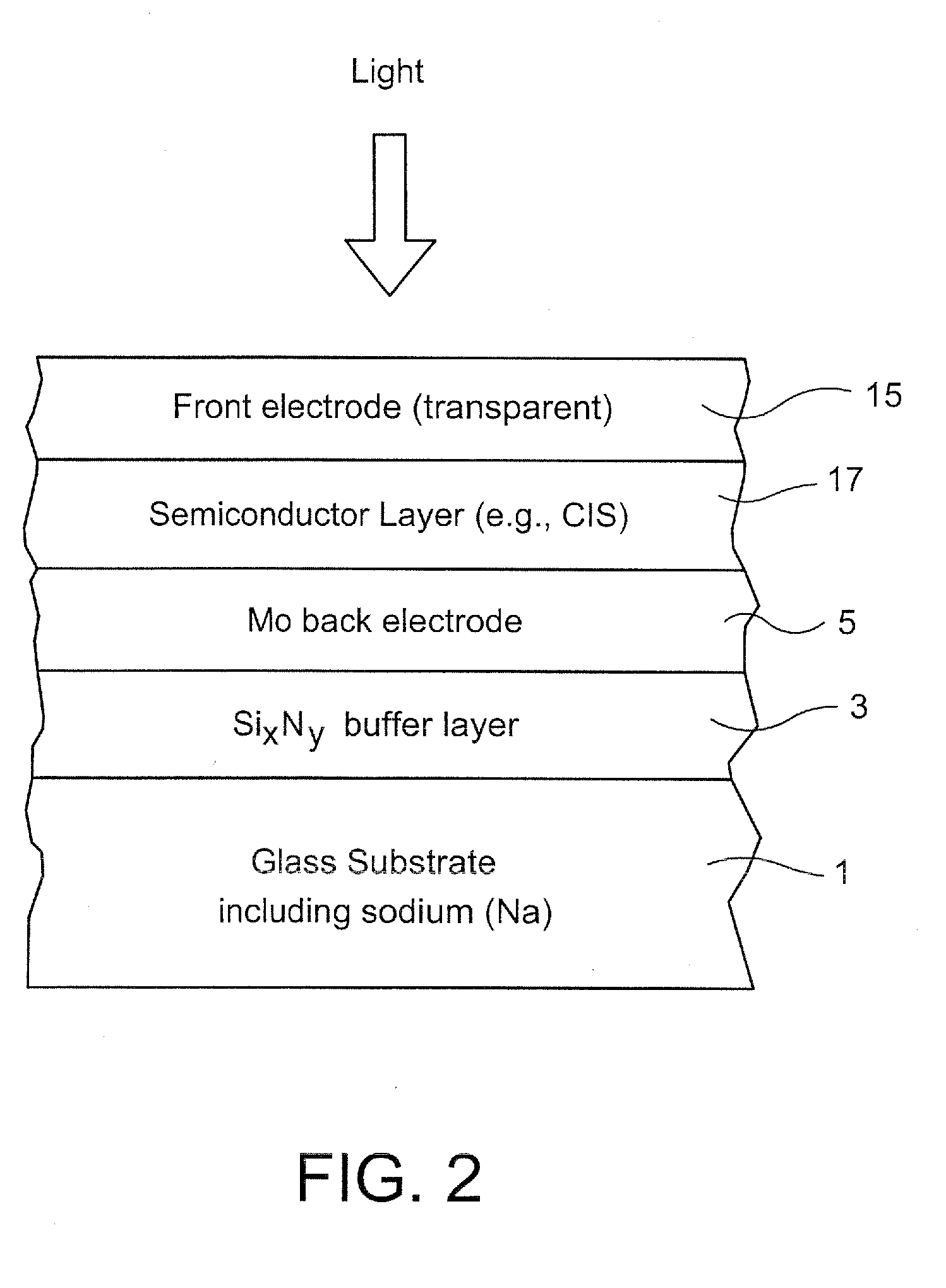
[0007]In certain example embodiments of this invention, an electrode structure is provided for use in solar cells and the like. In certain example embodiments, an electrode structure includes a supporting glass substrate (e.g., soda-lime silica based float glass), a buffer layer (e.g., SixNy), and a conductive electrode (e.g., Mo) provided in this order. The buffer layer is advantageous in that it prevents or reduces sodium (Na) migration from the glass substrate, through the Mo back electrode, and into semiconductor layer(s) of the electronic device (e.g., solar cell or other suitable electronic device). Thus, if desired, sodium may be added to the semiconductor layer from above in a post-deposition treatment (i.e., not from the glass). The buffer layer may be of silicon nitride, and may include oxygen and / or other element(s) as well in certain example embodiments of this invention. The buffer layer may be made up of a single layer or multiple layers in different example embodiments of this invention.
[0009]Other example advantages of the buffer layer relate to better control of the mechanical and / or efficiency properties of the electrode layer and / or electronic device. The Mo electrode layer acts as a nucleation layer for the CIS / CIGS stack in certain example embodiments. By controlling the deposition parameters of the buffer layer, it is possible to achieve the desired properties of the Mo electrode layer and in turn to also achieve a desired degree of selenization of the absorber layer, and so forth. The high line speed and deposition pressures used in sputtering vacuum coaters are also favorable in producing a more open metal (e.g., Mo) surface, resulting in a better adhesion between the absorber and Mo to form a MoSe2-xOx transition layer at the Mo / absorber interface, which is optional in certain example embodiments of this invention. This MoSe2-x Ox transition layer at the Mo / absorber interface in certain example embodiments of this invention contributes to higher efficiencies of the CIS or CIGS layer.

Problems solved by technology

Unfortunately, such heat treating temperatures often cause diffusion of Na from the glass substrate into the coating in an uncontrollable and predictable manner.
This means that uncontrolled and unpredictable amounts of sodium can diffuse from the glass substrate into a CIGS or CIS layer in a solar cell or other electronic device, which can lead to undesirable and / or unpredictable functionality in certain instances.

Method used


Image

  • Electrode structure for use in electronic device and method of making same
  • Electrode structure for use in electronic device and method of making same
  • Electrode structure for use in electronic device and method of making same

Examples


Embodiment Construction

[0007]In certain example embodiments of this invention, an electrode structure is provided for use in solar cells and the like. In certain example embodiments, an electrode structure includes a supporting glass substrate (e.g., soda-lime silica based float glass), a buffer layer (e.g., SixNy), and a conductive electrode (e.g., Mo) provided in this order. The buffer layer is advantageous in that it prevents or reduces sodium (Na) migration from the glass substrate, through the Mo back electrode, and into semiconductor layer(s) of the electronic device (e.g., solar cell or other suitable electronic device). Thus, if desired, sodium may be added to the semiconductor layer from above in a post-deposition treatment (i.e., not from the glass). The buffer layer may be of silicon nitride, and may include oxygen and / or other element(s) as well in certain example embodiments of this invention. The buffer layer may be made up of a single layer or multiple layers in different example embodiment...


PUM

PropertyMeasurementUnit
thickaaaaaaaaaa
thickaaaaaaaaaa
thickaaaaaaaaaa

Abstract

An electrode structure is provided for use in an electronic device. In certain example embodiments, an electrode structure includes a supporting glass substrate (e.g., soda-lime silica based float glass), a buffer layer (e.g., SixNy), and a conductive electrode (e.g., Mo) provided in this order. The buffer layer is advantageous in that it prevents or reduces sodium (Na) migration from the glass substrate into semiconductor layer(s) of the electronic device.

Description

[0001]This invention relates to an electrode structure for use in an electronic device. In certain example embodiment, an electrode structure includes a supporting glass substrate (e.g., soda-lime silica based float glass), a buffer layer (e.g., SixNy), and a conductive electrode (e.g., Mo) provided in this order. The buffer layer is advantageous in that it prevents or reduces sodium (Na) migration from the glass substrate into semiconductor layer(s) of the electronic device (e.g., solar cell or other suitable electronic device). A method of making the same is also provided.BACKGROUND OF THE INVENTION[0002]Back electrodes for solar cells and the like are known in the art. For example and without limitation, see U.S. Patent Document Nos. 2004 / 0261841, 2005 / 0253142, U.S. Pat. No. 5,981,868, 2005 / 0236032, U.S. Pat. No. 5,477,088, 2005 / 0186342, 2005 / 0257825, 2005 / 0284518, 2004 / 0087172, and 2005 / 0072461, the disclosures of which are hereby incorporated herein by reference.[0003]Back elec...

Claims


Application Information

Patent Timeline
Patent Type & Authority Applications(United States)
IPC IPC(8): H01L31/0224
CPCH01L31/022425Y02E10/541H01L31/0392H01L31/0322H01L31/03923Y02P70/50
Inventor KRASNOV, ALEXEY
Owner GUARDIAN GLASS LLC
Learn More