
Graphene sheet and method for producing the same

Active Publication Date: 2012-08-02
KYUSHU UNIV
View PDF1 Cites 49 Cited by
  • Summary
  • Abstract
  • Description
  • Claims
  • Application Information

AI Technical Summary

Benefits of technology

[0035]According to the invention, by using a relatively inexpensive single crystal substrate, such as sapphire (α-Al2O3), MgO or quartz, a metal film raw material is sputtered on the single crystal substrate at a high temperature, thereby growing epitaxially a metal film from the surface of the single crystal substrate, and by using the substrate having the epitaxial metal film formed thereon, a carbon material is reacted by making in contact with the surface of the metal film. Consequently, a gra

Problems solved by technology

For providing a graphene sheet, a method of mechanically exfoliated from graphite, such as HOPG, with a Scotch adhesive tape has been practiced, but resulting graphene sheets are fluctuated in size and thickness, and cannot be subjected to practical applications.
However, there are problems that the SiC single crystal substrate and an Ni (111) single crystal substrate used in these methods are expensive, and are available only in a limited size.

Method used


Image

  • Graphene sheet and method for producing the same
  • Graphene sheet and method for producing the same
  • Graphene sheet and method for producing the same

Examples


first embodiment

[0087]In the invention, a graphene sheet is grown by making a carbon material into contact with an epitaxial metal film that is formed on a surface of a single crystal substrate.

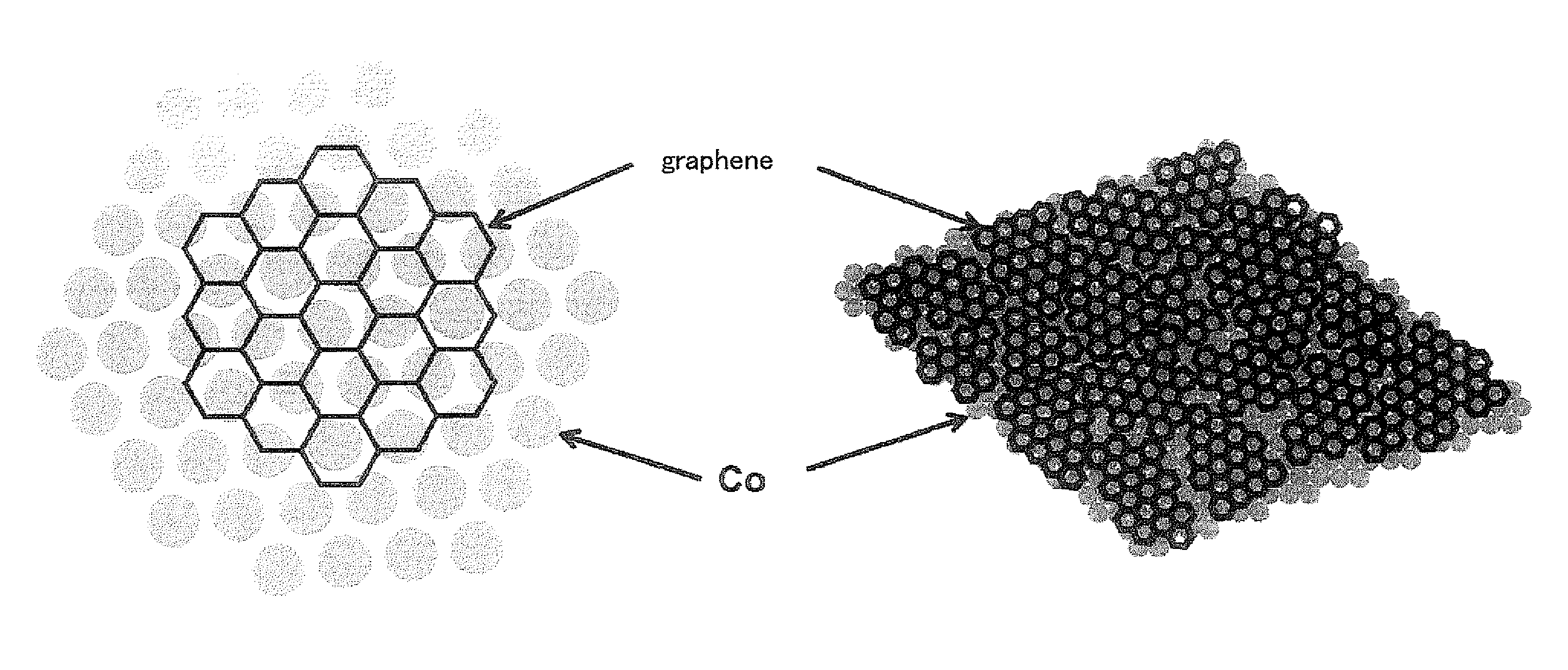
[0088]In one embodiment of the graphene sheet obtained by the method, the graphene sheet contains a large number of graphene domains, the domains each have an area of from 0.000001 μm2 to 100,000 mm2, preferably from 0.000001 μm2 to 50,000 mm2, and more preferably from 0.000001 μm2 to 100 mm2, and orientations of 6-membered rings in the domains are averagely aligned in a single direction over the graphene sheet.

[0089]The language “orientations of 6-membered rings in the domains are averagely aligned in a single direction over the graphene sheet” includes such a state that a LEED (low energy electron diffraction) image of a substrate having the graphene sheet formed thereon has six equally spaced diffraction spots, or the spots with a certain width, or has a ring diffraction pattern having locally distributed...

second embodiment

[0119]In one embodiment of the graphene sheet of the invention, a graphene sheet having a triangular, rectangular, hexagonal, octagonal or circular planar shape having an area of from 0.0001 to 1,000,000 μm2, and a graphene sheet having a planar shape having an edge with a zigzag structure or an armchair structure are provided.

[0120]The graphene sheet may be synthesized on a surface of an epitaxial metal film by making a carbon material into contact with the surface of the metal film, as described above for the first embodiment. Typically, pits having a rectangular shape or a triangular shape are formed on the epitaxial film upon heating, and the graphene sheet is formed dominantly in the pits. Accordingly, the graphene sheet of the invention may have a characteristic shape, such as a rectangular shape and a triangular shape. The graphene sheet may have the aforementioned planer shape having an area of from 0.0001 to 1,000,000 μm2, and preferably from 0.001 to 10,000 μm2, and the th...

example 1

[0133]Graphene was synthesized by a CVD method. A horizontal tubular furnace was used, and a single crystal substrate having a catalyst metal formed as a film thereon was placed at the center of the quartz tube mounted on the tubular furnace. A magnet was attached to an end of the specimen support of the substrate, and the substrate as the specimen was slid between a high temperature zone and a low temperature zone of an electric furnace with a magnet outside the quartz tube of the electric furnace, thereby performing quenching and the like of the specimen.

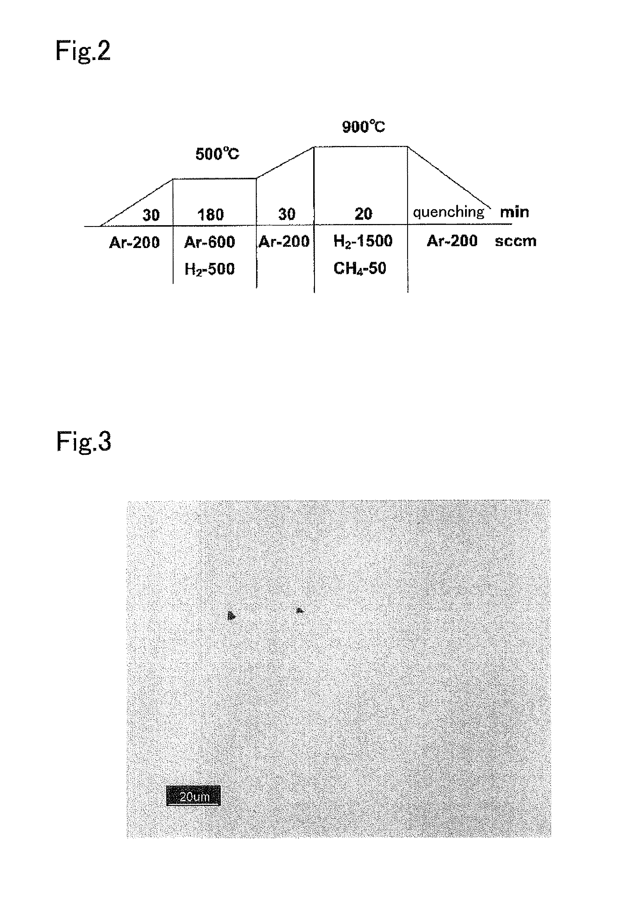
[0134]The Co / c-plane sapphire or Ni / c-plane sapphire produced in the aforementioned manner was used as the substrate. Methane gas was used as a carbon material, and hydrogen annealing at 500° C. was performed for the substrate in the quartz tube before CVD synthesis at 900° C. The standard condition of temperature and gas used from the heating step to the cooling step is shown in FIG. 2.

[0135]Under the standard condition shown in ...


PUM

PropertyMeasurementUnit
Fractionaaaaaaaaaa
Fractionaaaaaaaaaa
Fractionaaaaaaaaaa

Abstract

To provide a graphene sheet that has a large area, is homogeneous, and has a small amount of domain boundaries, a novel method for producing a graphene sheet suitable for industrial applications, such as application to electronics, that is capable of producing a graphene sheet that has well aligned crystal orientation at a low cost, and a graphene sheet.In the method for producing a graphene sheet of the present invention, a substrate containing a single crystal substrate having formed on the surface thereof an epitaxial metal film is used, and a graphene sheet is grown by making a carbon material into contact with the surface of the epitaxial metal film. In the graphene sheet of the present invention, the graphene sheet is constituted by a number of graphene domains, the domains each have an area of from 0.000001 μm2 to 100,000 mm2, and the orientations of 6-membered rings in the domains are averagely aligned in a single direction over the graphene sheet.

Description

TECHNICAL FIELD[0001]The present invention relates to a graphene sheet and a method for producing the same, and more specifically a graphene sheet and a method for producing the same using a metal film as a catalyst.BACKGROUND ART[0002]Graphene is a single sheet or plural sheets taken out from graphite, and has an ideal two-dimensional structure constituted by sp2 carbon. Graphene is referred to as single layer graphene, two-layer graphene, multi-layer graphene, and the like, depending on the number of layers.[0003]Graphene has been reported to have a considerably high mobility of electrons and holes (from 10,000 to 200,000 cm2 / Vs), and the mobility exceeds silicon, GaAs and the like. Graphene is in the form of a two-dimensional sheet and thus can be applied with production techniques for semiconductors, such as lithography and etching, thereby providing various structures. Furthermore, graphene has excellent transparency and mechanical flexibility, and possibly has applications to ...

Claims


Application Information

Patent Timeline
IPC IPC(8): B32B15/04B32B9/00C23C16/26C01B31/00B82Y30/00B82Y40/00
CPCB82Y30/00B82Y40/00C01B31/0461C01B2204/02Y10T428/26C01B2204/32Y10T428/24777Y10T428/21C01B2204/04C01B32/188Y10T428/31678
Inventor AGO, HIROKIITO, YOSHITOTANAKA, IZUMIMIZUNO, SEIGITSUJI, MASAHARU
Owner KYUSHU UNIV
Learn More