Non-volatile memory device and method for fabricating the same
- Summary
- Abstract
- Description
- Claims
- Application Information
AI Technical Summary
Benefits of technology
Problems solved by technology
Method used
Image

Examples
first embodiment
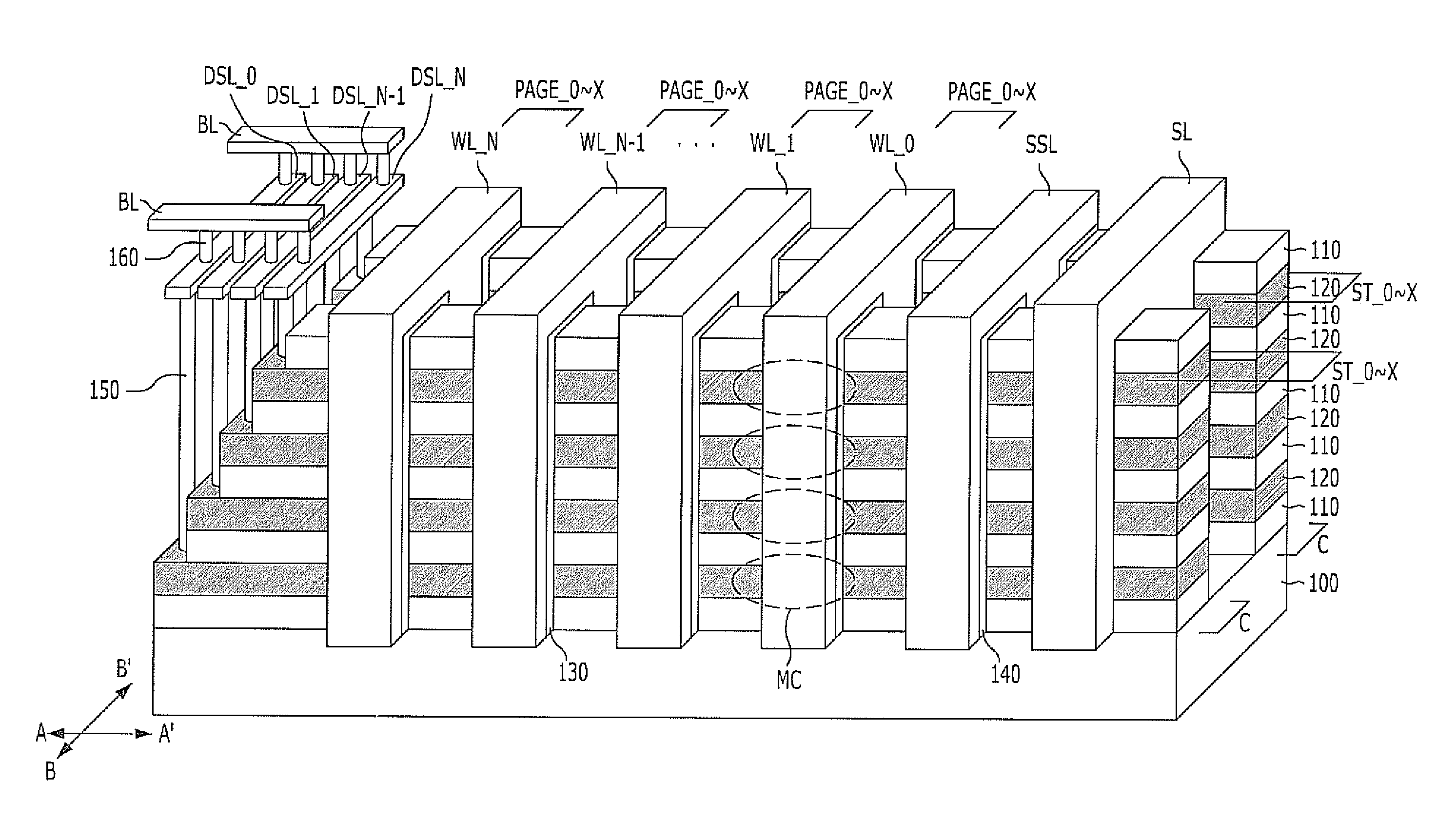
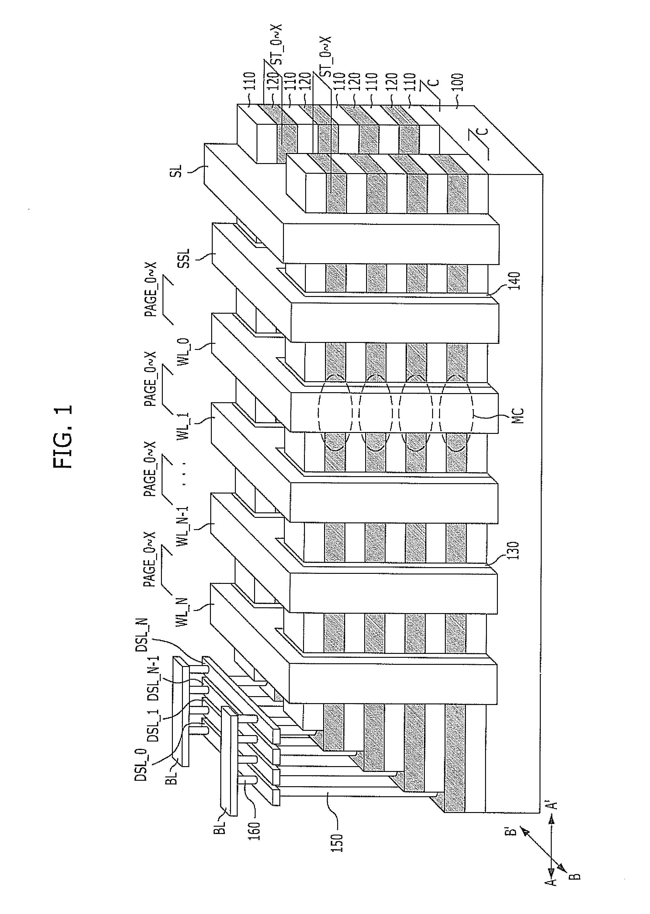
[0041]Referring to FIG. 2E, the non-volatile memory device in accordance with the present invention includes a substrate 200, channel structures 210A, a source line SL, source selection lines SSL, and a plurality of word lines WL_0 to WL_N. The substrate 200 includes low-resistance resistors 204 having a lower resistance than the source line SL. The channel structure 210A is extended in a first direction and includes inter-layer dielectric layers 212 and channel layers 214 that are stacked alternately over the substrate 200. The source line SL is extended in a second direction while contacting the sidewall of the channel structure 210A and the lower end of the source line SL contacts the low-resistance resistors 204. The source selection lines SSL is symmetrically disposed on both sides of the source line SL and extended in the second direction while contacting the sidewall of the channel structure 210A with a gate insulation layer 140 (see FIG. 1) between them. The word lines WL_0 ...
second embodiment
[0068]Referring to FIG. 3E, the non-volatile memory device in accordance with the present invention includes a substrate 300, channel structures 310A, a source line SL, source selection lines SSL, a plurality of word lines WL_0 to WL_N, metal lines M, and contacts 335, 385, PD and 395. Each channel structures 310A is extended in a first direction and includes inter-layer dielectric layers 312 and channel layers 314 that are stacked alternately over the substrate 300. The source line SL is extended in a second direction and contacts the sidewalls of the channel structures 310A. The source selection lines SSL are symmetrically disposed on both sides of the source line SL and extended in the second direction and contact the sidewalls of the channels structure 310A with a gate insulation layer 140 (see FIG. 1) between them. The word lines WL_0 to WL_N are symmetrically disposed on both sides of the source selection lines SSL and extended in the second direction and contact the sidewalls...
third embodiment
[0097]Referring to FIG. 4E, the non-volatile memory device in accordance with the present invention includes a substrate 400, a peripheral circuit gate 402, which is a peripheral circuit device disposed over the substrate 400, a fourth insulation layer 406 covering the peripheral circuit gate 402, channel structures 410A, a source line SL, source selection lines SSL, and a plurality of word lines WL_0 to WL_N. Each channel structure 410A is extended in a first direction and includes inter-layer dielectric layers 412 and channel layers 414 that are stacked alternately over the fourth insulation layer 406. The source line SL is extended in a second direction and contacts the sidewalls of the channel structures 410A, and the lower end of the source line SL is coupled with the peripheral circuit gate 402. The source selection lines SSL are symmetrically disposed on both sides of the source line SL and extended in the second direction while contacting the sidewalls of the channel structu...
PUM
 Abstract
Description
Claims
Application Information
 - R&D Engineer
- R&D Manager
- IP Professional
- Industry Leading Data Capabilities
- Powerful AI technology
- Patent DNA Extraction
Browse by: Latest US Patents, China's latest patents, Technical Efficacy Thesaurus, Application Domain, Technology Topic.
© 2024 PatSnap. All rights reserved.Legal|Privacy policy|Modern Slavery Act Transparency Statement|Sitemap