Hierachically-modular nanoelectronic differential amplifiers, op amps, and associated current sources utilizing carbon nanotubes, graphene nanoribbons, printed electronics, polymer semiconductors, or other related materials

Active Publication Date: 2011-12-01
GULA CONSULTING LLC
View PDF10 Cites 7 Cited by
  • Summary
  • Abstract
  • Description
  • Claims
  • Application Information

AI Technical Summary

Benefits of technology

[0010]For purposes of summarizing, certain aspects, advantages, and novel features are described herein. Not all such advantages may be achieved in accordance with any one particular embodiment. Thus, th

Problems solved by technology
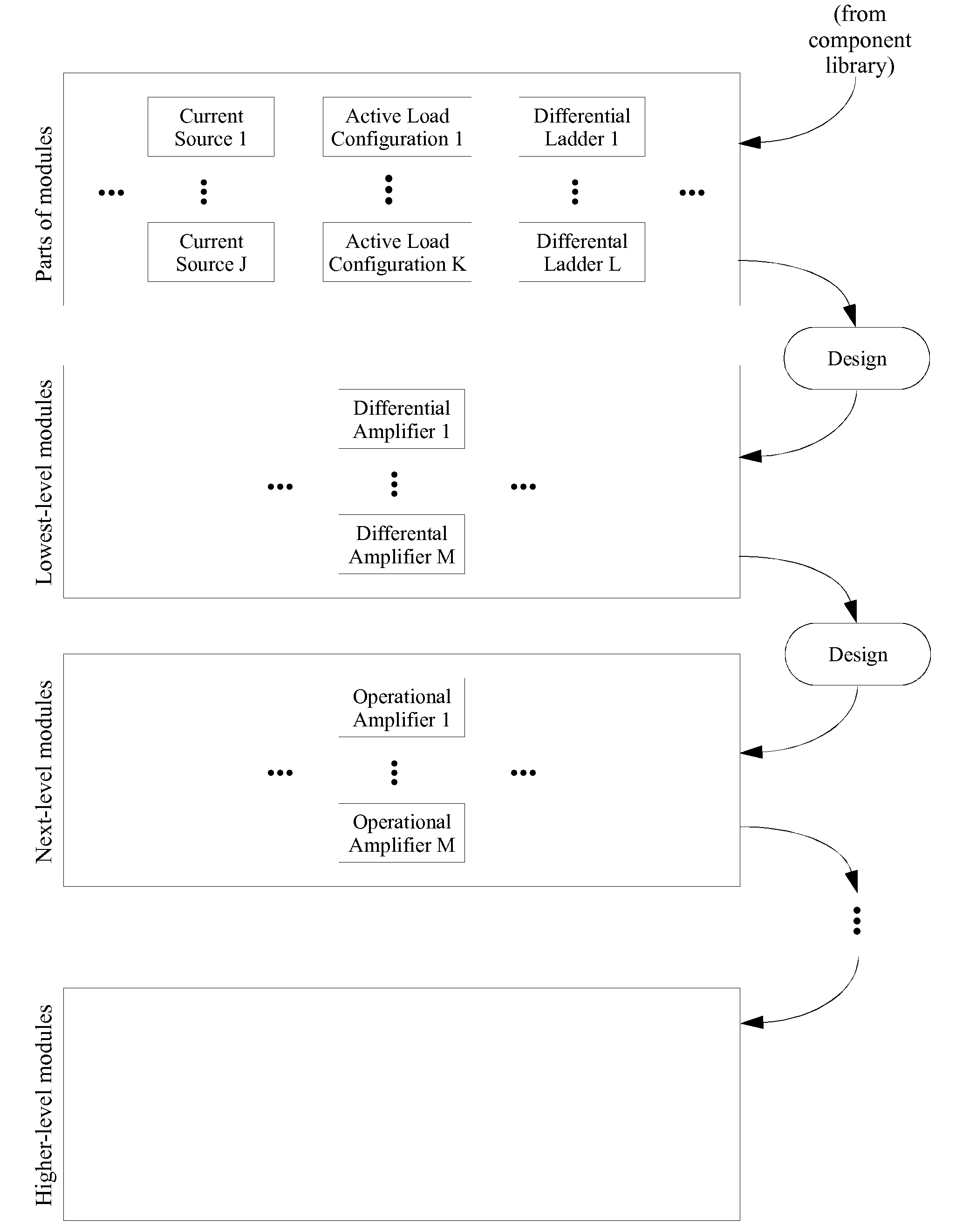
However, with poor electrical interfacing to the larger-scale world, the valuable gifts and opportunities offered by the sensitivities and signal integrity of these nanoscale devices is easily (and perhaps literally) would otherwise be lost in the noise.

Method used


Image

  • Hierachically-modular nanoelectronic differential amplifiers, op amps, and associated current sources utilizing carbon nanotubes, graphene nanoribbons, printed electronics, polymer semiconductors, or other related materials
  • Hierachically-modular nanoelectronic differential amplifiers, op amps, and associated current sources utilizing carbon nanotubes, graphene nanoribbons, printed electronics, polymer semiconductors, or other related materials
  • Hierachically-modular nanoelectronic differential amplifiers, op amps, and associated current sources utilizing carbon nanotubes, graphene nanoribbons, printed electronics, polymer semiconductors, or other related materials

Examples


Embodiment Construction

[0094]In the following, numerous specific details are set forth to provide a thorough description of various embodiments. Certain embodiments may be practiced without these specific details or with some variations in detail. In some instances, certain features are described in less detail so as not to obscure other aspects. The level of detail associated with each of the elements or features should not be construed to qualify the novelty or importance of one feature over the others.

[0095]In the following description, reference is made to the accompanying drawing figures which form a part hereof, and which show by way of illustration specific embodiments of the invention. It is to be understood by those of ordinary skill in this technological field that other embodiments may be utilized, and structural, electrical, as well as procedural changes may be made without departing from the scope of the present invention.

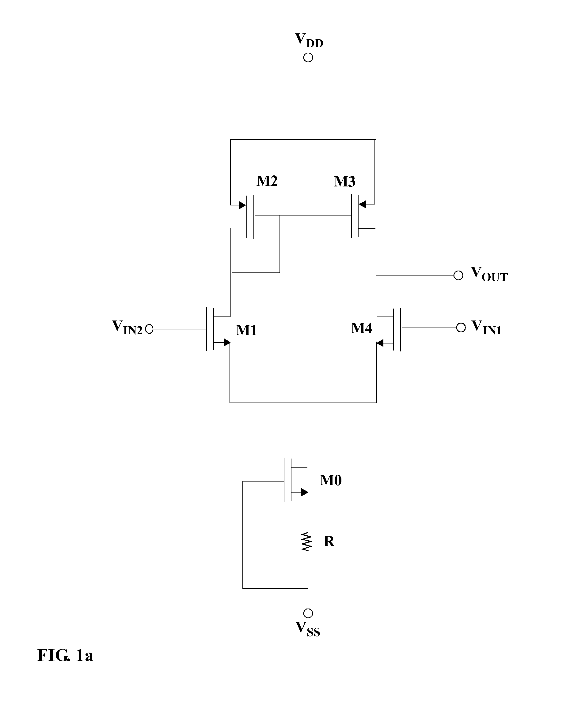
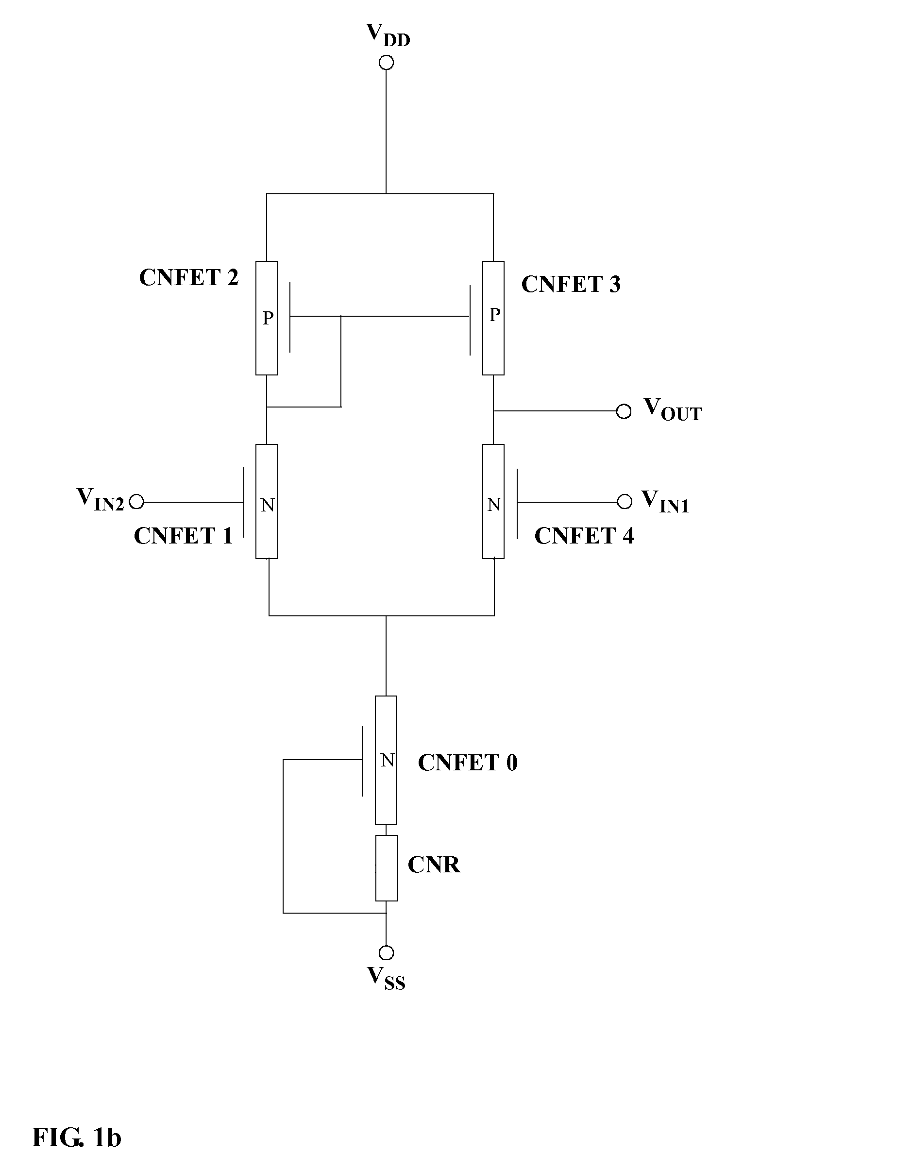
[0096]For carbon nanotube and other nanotechnology sensors and transduc...


PUM


Abstract

A method for implementing electronic circuit modules on elongated structures of semiconducting materials such as carbon nanotubes, graphene nanoribbons, elongated structures of semiconducting polymers or organic semiconductors, other related materials, and printed electronics strip structures is disclosed. The method provides that a plurality of modules can be implemented on distinct adjacent portions of the same elongated structure of semiconducting materials. In powering the modules, each circuit comprises a chain of electronic components arranged so that each end of the chain can function as a power supply terminal. Larger electronic circuit modules can be created from smaller module, and. such a modular hierarchy may be extended to an arbitrary number of levels. In a Computer Aided Design (CAD) applications for nanoelectronics and printed electronics, designs for hierarchies electronic circuit modules can be stored and retrieved from one or more a libraries of circuit designs.

Description

CROSS-REFERENCE TO RELATED APPLICATIONS[0001]Pursuant to 35 U.S.C. §119(e), this application claims benefit of priority from Provisional U.S. Patent application Ser. No. 61 / 348,366, filed May 26, 2010, the contents of which are incorporated by reference.COPYRIGHT & TRADEMARK NOTICES[0002]A portion of the disclosure of this patent document may contain material, which is subject to copyright protection. Certain marks referenced herein may be common law or registered trademarks of the applicant, the assignee or third parties affiliated or unaffiliated with the applicant or the assignee. Use of these marks is for providing an enabling disclosure by way of example and shall not be construed to exclusively limit the scope of the disclosed subject matter to material associated with such marks.BACKGROUND OF THE INVENTION[0003]The present invention generally relates to nanotechnology, and in particular, to differential amplifiers, current sources, and associated circuits created from carbon ...

Claims


Application Information

Patent Timeline
IPC IPC(8): G06F17/50
CPCB82Y10/00G06F17/5063H01L27/0207H01L51/0558H01L29/0673H01L51/0048H01L27/092G06F30/36H10K85/221H10K10/484
Inventor LUDWIG, LESTER F.
Owner GULA CONSULTING LLC
Why Eureka
Try Eureka