Liquid crystal display device
a liquid crystal display and display device technology, applied in non-linear optics, instruments, optics, etc., can solve the problems of display defect, low alignment stability of photo-alignment methods compared with rubbing processes, and brightness and chromaticity, so as to prevent yellow shift on the display and suppress the dc afterimage
- Summary
- Abstract
- Description
- Claims
- Application Information
AI Technical Summary
Benefits of technology
Problems solved by technology
Method used
Image
Examples
first embodiment
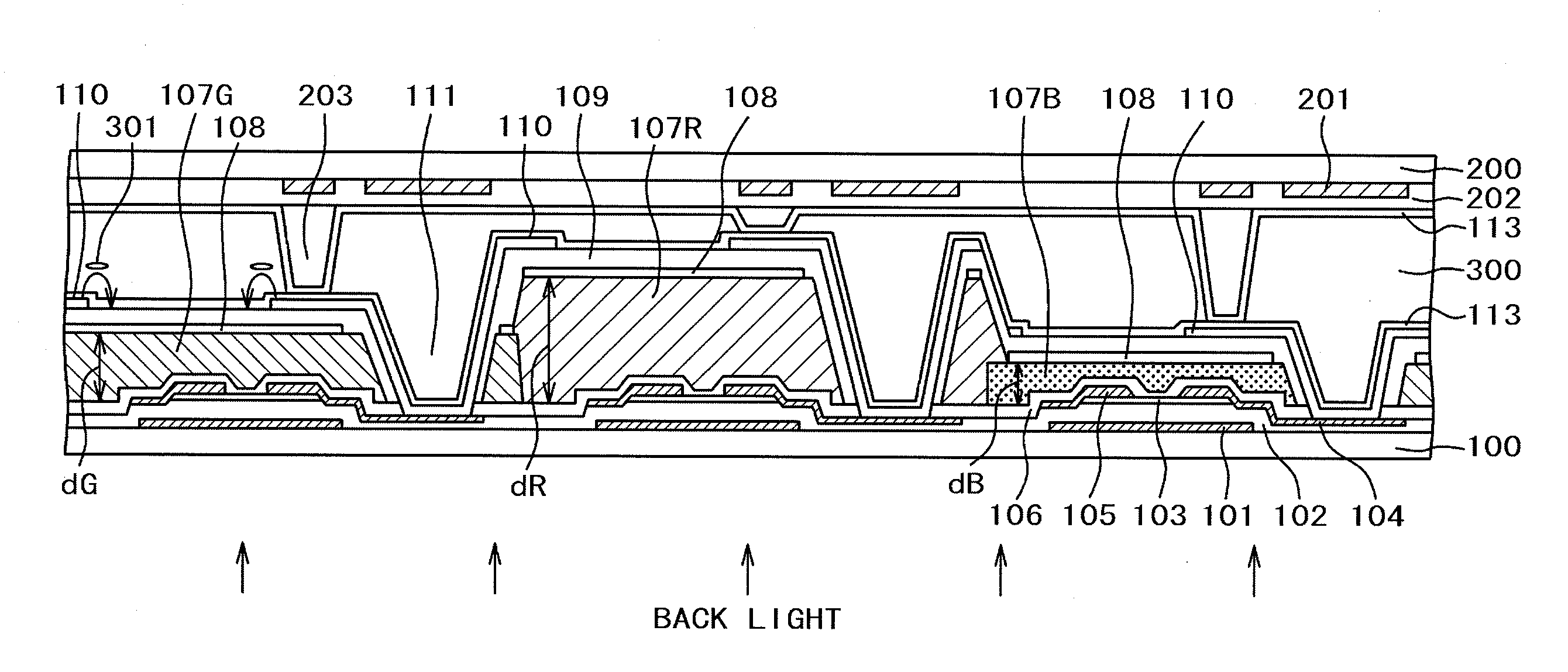
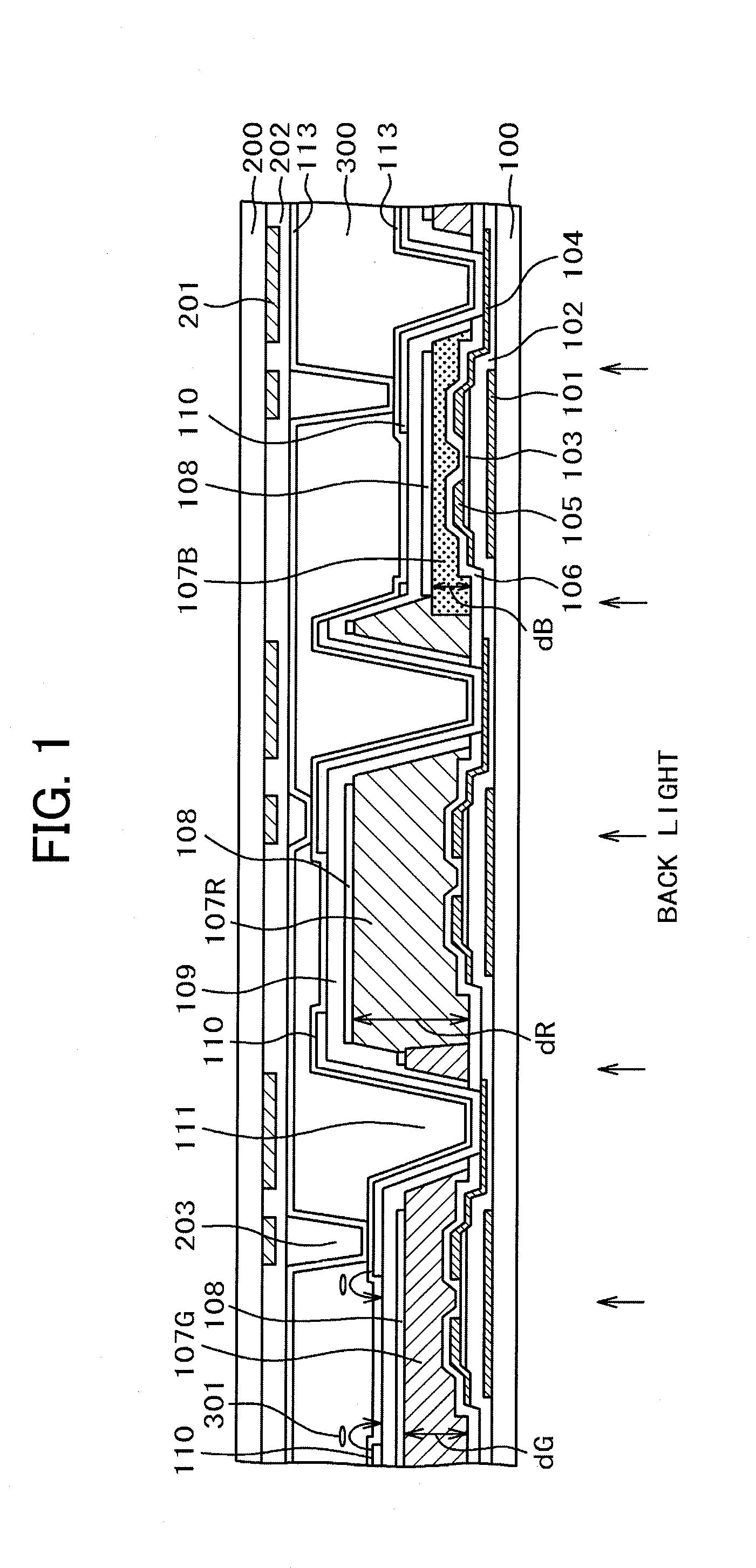
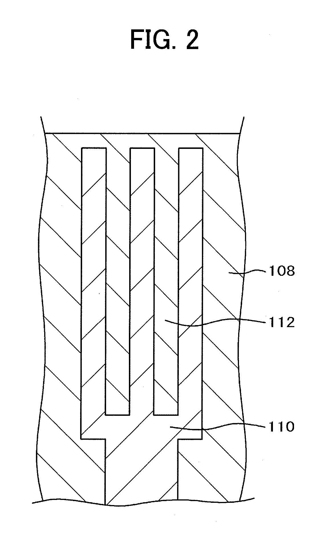
[0027]FIG. 1 is a sectional view of a liquid crystal display panel according to a first embodiment of the present invention. FIG. 1 illustrates the IPS of the COA type in which pixels provided with TFTs, opposed electrodes 108, pixel electrodes 110, and color filters 107R, 107G and 107B are formed on a TFT substrate 100 in matrix.
[0028]As FIG. 1 shows, alignment films 113 are formed on surfaces of the TFT substrate 100 and an opposed substrate 200 which face a liquid crystal layer 300. The material with higher photoconductivity than for the generally employed liquid crystal display panel is used for forming each of the respective alignment films 113 formed at both sides of the TFT substrate 100 and the opposed substrate 200, respectively for coping with the DC afterimage characteristic. In other words, the material having the electric resistance largely reduced by low light intensity is used for forming the alignment film. As the material with photoconductivity for forming the align...
second embodiment
[0058]FIG. 7 is a sectional view of a liquid crystal display panel according to the second embodiment of the present invention. The present embodiment provides COA intended to prevent color shift on the display while suppressing the DC afterimage. Referring to FIG. 7, the color filters 107R, 107G, and 107B are provided on the TFT substrate 100 to form the COA structure. Arrows shown in FIG. 7 denote light rays from the back light.
[0059]In FIG. 7, the material with high photoconductivity is used for forming the alignment film 113. Its photoconductivity is higher than that of the alignment film used for the liquid crystal panel as the generally employed structure. This makes it possible to reduce electric resistance of the alignment film 113 in operation, thus suppressing the DC afterimage.
[0060]The alignment film 113 shown in FIG. 7 has its transmittance reduced at the short wavelength side likewise the case described referring to FIGS. 3 and 4. If intensity of the light input to eac...
PUM
 Abstract
Description
Claims
Application Information
 - R&D
- Intellectual Property
- Life Sciences
- Materials
- Tech Scout
- Unparalleled Data Quality
- Higher Quality Content
- 60% Fewer Hallucinations
Browse by: Latest US Patents, China's latest patents, Technical Efficacy Thesaurus, Application Domain, Technology Topic, Popular Technical Reports.
© 2025 PatSnap. All rights reserved.Legal|Privacy policy|Modern Slavery Act Transparency Statement|Sitemap|About US| Contact US: help@patsnap.com


