Manufacturing method for glass substrate with thin film
a manufacturing method and technology of glass substrate, applied in glass making apparatus, manufacturing tools, instruments, etc., can solve the problems of glass substrate warping and membrane stress
- Summary
- Abstract
- Description
- Claims
- Application Information
AI Technical Summary
Benefits of technology
Problems solved by technology
Method used
Image


Examples
first embodiment
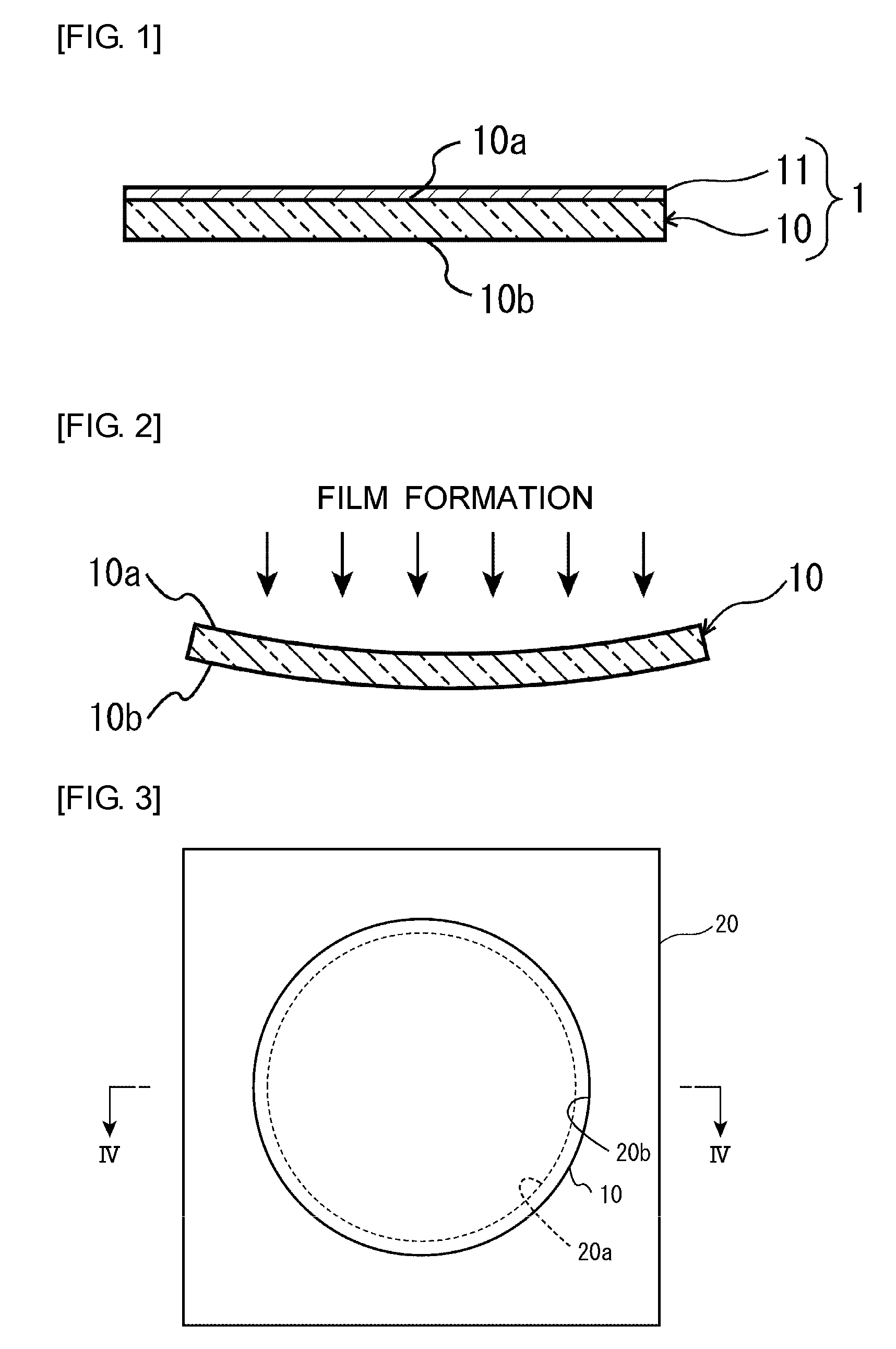
[0031]FIG. 1 is a cross-sectional view of a glass substrate 1 with a thin film to be manufactured in this embodiment. First, the structure of a glass substrate 1 with a thin film will be described with reference to FIG. 1.
[0032]As shown in FIG. 1, the glass substrate 1 with a thin film includes a glass substrate 10. The glass substrate 10 can be appropriately selected according to the characteristics of the glass substrate 1 with a thin film or other factors. The glass substrate 10 can be formed, for example, of a borosilicate glass substrate.
[0033]The glass substrate 10 has first and second principal surfaces 10a and 10b parallel to each other. Each of the first and second principal surfaces 10a and 10b is flat. A thin film 11 is formed on the first principal surface 10a. The thin film 11 can be appropriately selected according to the characteristics of the glass substrate 1 with a thin film or other factors. For example, if the glass substrate 1 with a thin film is an IR cutoff fi...
second embodiment
[0063]The first embodiment has described the case where a thin film 11 is formed in a single layer. However, the manufacturing method for a glass substrate with a thin film according to the present invention is applicable to the case where a thin-film stack including a plurality of thin films deposited one on another is formed on the principal surface 10a, 10b of the glass substrate 10. In this case, the membrane stress applied to the glass substrate during the cooling process is likely to be large as compared to the case where the thin film 11 is formed in a single layer. Therefore, the resultant glass substrate with a thin film tends to be largely warped. Hence, it is effective to apply to this case the manufacturing method for a glass substrate with a thin film according to the present invention.
[0064]Specific examples of the thin-film stack include multilayers formed by alternately depositing high-refractive index films, such as ZrO2 films, TiO2 films or Nb2O2 films, and low-ref...
third embodiment
[0065]The above embodiments have described the cases where a thin film 11 is formed only on one principal surface 10a of the glass substrate 10. However, the present invention is not limited to this structure.
[0066]FIG. 7 is a cross-sectional view of a glass substrate 1 with a thin film according to this embodiment. As shown in FIG. 7, thin films 11a and 11b may be formed on both the first and second principal surfaces 10a and 10b, respectively, of the glass substrate 10. The manufacturing method for a glass substrate with a thin film according to the present invention can also suitably be applied to this case.
[0067]In this embodiment, one of the thin films 11a and 11b having a larger compressive stress in the direction along the surface thereof from after the formation of the thin film to the final state is formed on the convex principal surface, while the other thin film having a larger tensile stress is formed on the concave principal surface.
PUM
| Property | Measurement | Unit |
|---|---|---|
| Strain point | aaaaa | aaaaa |
| Temperature | aaaaa | aaaaa |
Abstract
Description
Claims
Application Information
 - R&D
- Intellectual Property
- Life Sciences
- Materials
- Tech Scout
- Unparalleled Data Quality
- Higher Quality Content
- 60% Fewer Hallucinations
Browse by: Latest US Patents, China's latest patents, Technical Efficacy Thesaurus, Application Domain, Technology Topic, Popular Technical Reports.
© 2025 PatSnap. All rights reserved.Legal|Privacy policy|Modern Slavery Act Transparency Statement|Sitemap|About US| Contact US: help@patsnap.com