Connecting module with optical indication
a technology of connecting modules and optical indications, applied in the direction of connection, electrical apparatus, coupling device connection, etc., can solve the problems of user confusion in identifying the correct connecting module or the correct connecting device, the limited space available in the host, and the inability to easily find and identify the number or symbol
- Summary
- Abstract
- Description
- Claims
- Application Information
AI Technical Summary
Benefits of technology
Problems solved by technology
Method used
Image
Examples
first embodiment
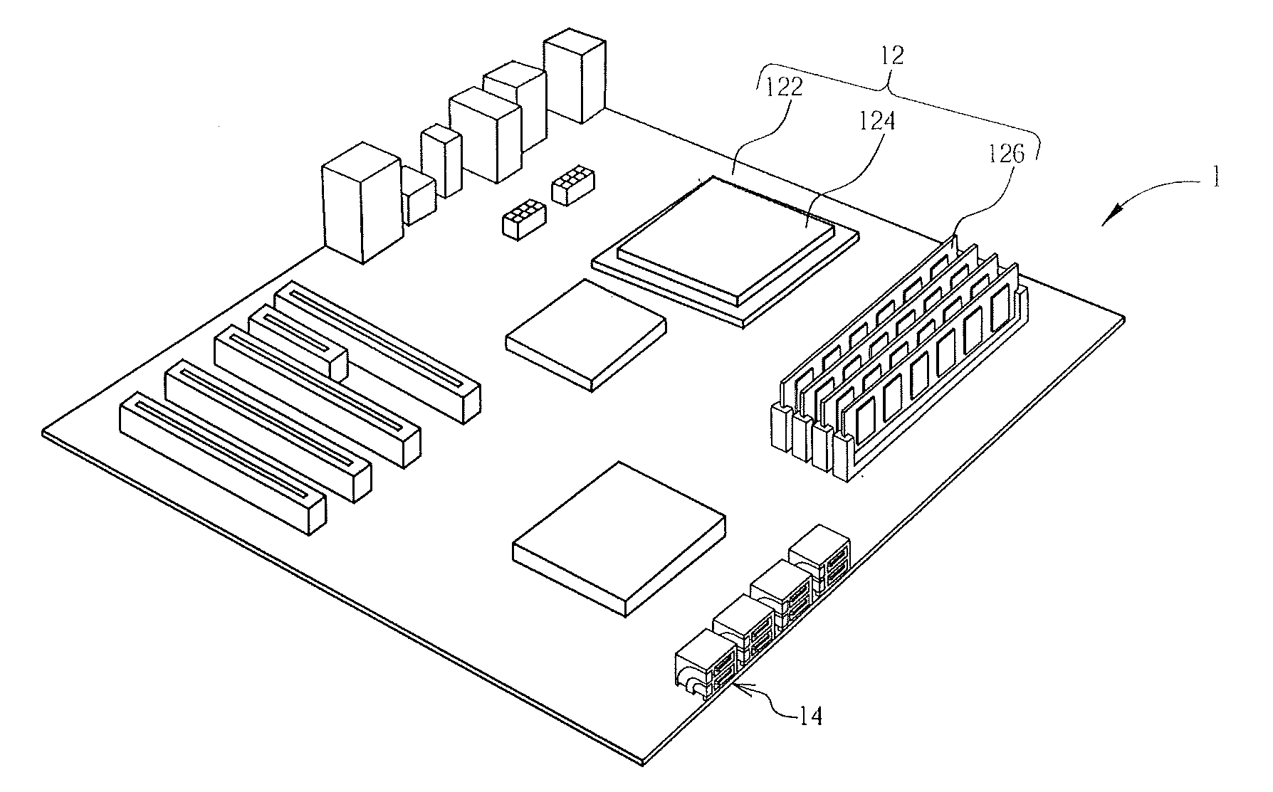
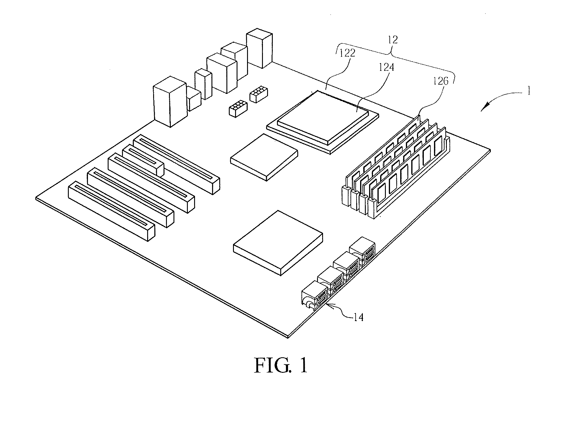
[0022]FIG. 1 is a schematic diagram showing an electronic device 1 in the invention. The electronic device 1 includes a processing module 12 and four connecting modules 14 electrically connected to the processing module 12. The processing module 12 includes a motherboard 122 and the elements on the motherboard such as a processor 124 and a memory 126. The connecting modules 14 are disposed on a motherboard 122 directly. In the embodiment, the connecting modules 14 are integrated connectors at the edge of the motherboard, and the invention is not limited thereto. The connecting modules 14 are disposed adjacently, and each connecting module 14 includes two first connectors piled with each other. Therefore, the electronic device 1 includes eight adjacent first connectors,
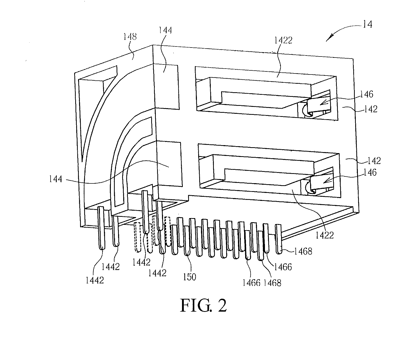
[0023]FIG. 2 is a three-dimensional diagram showing the connecting modules 14. FIG. 3 is a front view diagram showing the connecting module 14 in FIG. 2. FIG. 4 is a sectional diagram showing the connecting module 14 i...
second embodiment
[0025]In the embodiment of the invention, the switch 146 is disposed at the right side of the accommodating space 1422, but the invention is not limited thereto. For example, the switch 146 also may be disposed at the left side of the accommodating space 1422, and similarly, the elastic portion 1462 extends from the left side wall 1424 to the accommodating space 1422, which is shown as the dashed line in FIG. 3 and FIG. 4. As shown in FIG. 6, it is a sectional diagram showing the connecting module 14 taken along a line whose position is the same as the line Y-Y in FIG. 3 in the invention. In FIG. 6, the switch 146 is disposed at the bottom wall 1425 of the accommodating space 1422, and the elastic portion 1462 extends from the bottom wall 1426 to the accommodating space 1422. Similarly, after the plug 32 is inserted into the accommodating space 1422, the front portion of the plug 32 presses the elastic portion 1462 to contact the contacting portion 1464, and the switch 146 is also c...
third embodiment
[0027]In the above embodiment, the optical indicator 144 directly disposed adjacent to the first connector (near the opening of the accommodating space 1422) can directly indicate the needed first connector. To the sequentially arranged first connectors, if the corresponding optical indicators are also disposed sequentially, the user also may get the position of the needed connecting module according to the position of the optical indicator. As shown in FIG. 8 and FIG. 9, FIG. 8 is a three-dimensional diagram showing a connecting module 14 according to the invention, and FIG. 9 is a sectional diagram showing the first connector taken along a line whose position is the same as the line Y-Y in FIG. 3. The difference between FIG. 9 and FIG. 2 is that the optical indicators 144 are arranged on the housing 148 adjacently, and preferably located at the top wall of the housing 148 to allow the user to identify quickly. In addition, in the embodiment, the elastic portion 1462 of the switch ...
PUM
 Abstract
Description
Claims
Application Information
 - R&D
- Intellectual Property
- Life Sciences
- Materials
- Tech Scout
- Unparalleled Data Quality
- Higher Quality Content
- 60% Fewer Hallucinations
Browse by: Latest US Patents, China's latest patents, Technical Efficacy Thesaurus, Application Domain, Technology Topic, Popular Technical Reports.
© 2025 PatSnap. All rights reserved.Legal|Privacy policy|Modern Slavery Act Transparency Statement|Sitemap|About US| Contact US: help@patsnap.com


