Thin film balun
a thin film balun and balun technology, applied in the field of balun, can solve the problems of increasing the effective capacitance of the unbalanced circuit side, and achieve the effects of improving the passage characteristics of the thin film balun, excellent passage characteristics, and changing the character of the entire circui
- Summary
- Abstract
- Description
- Claims
- Application Information
AI Technical Summary
Benefits of technology
Problems solved by technology
Method used
Image
Examples
first embodiment
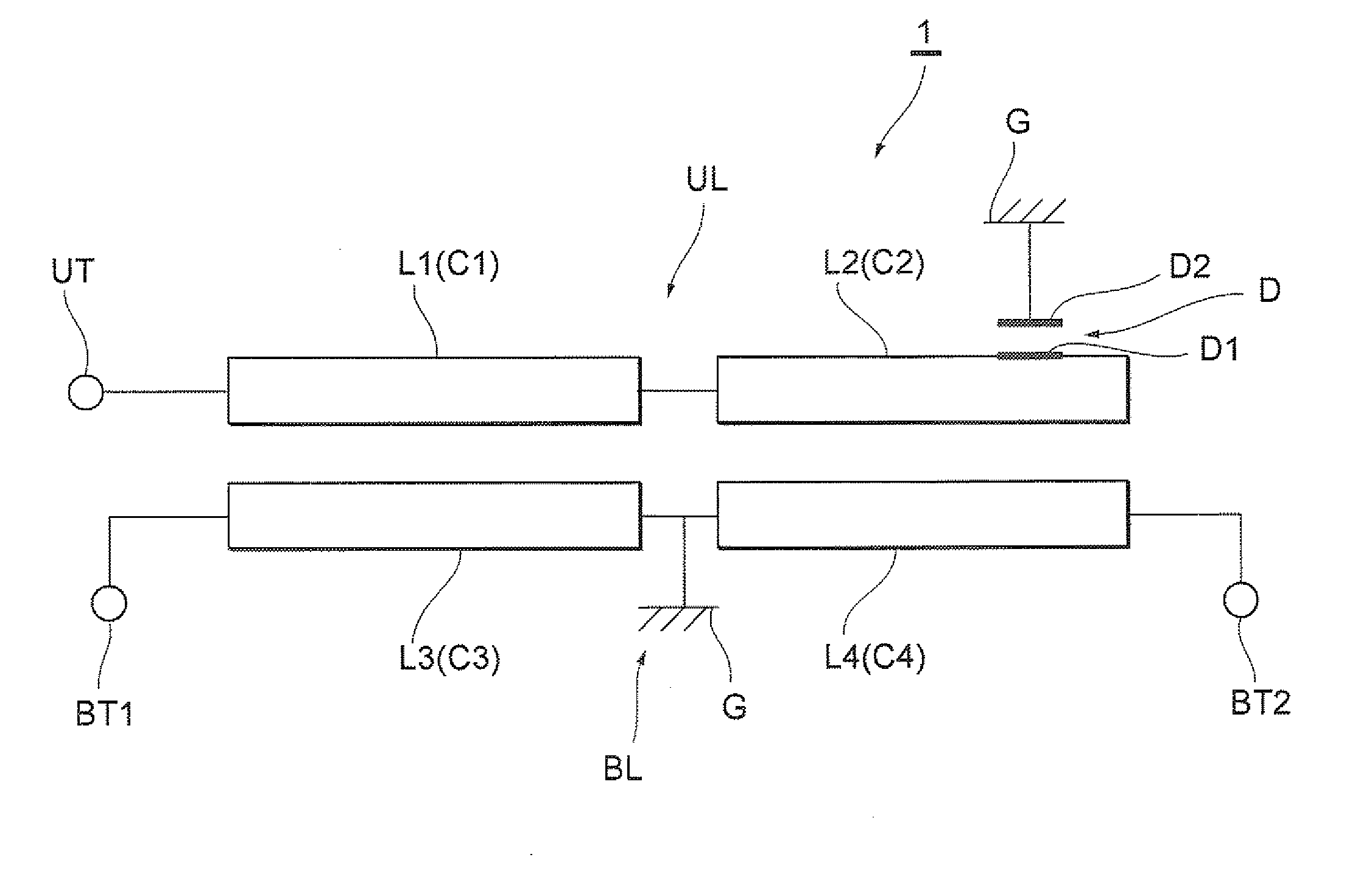
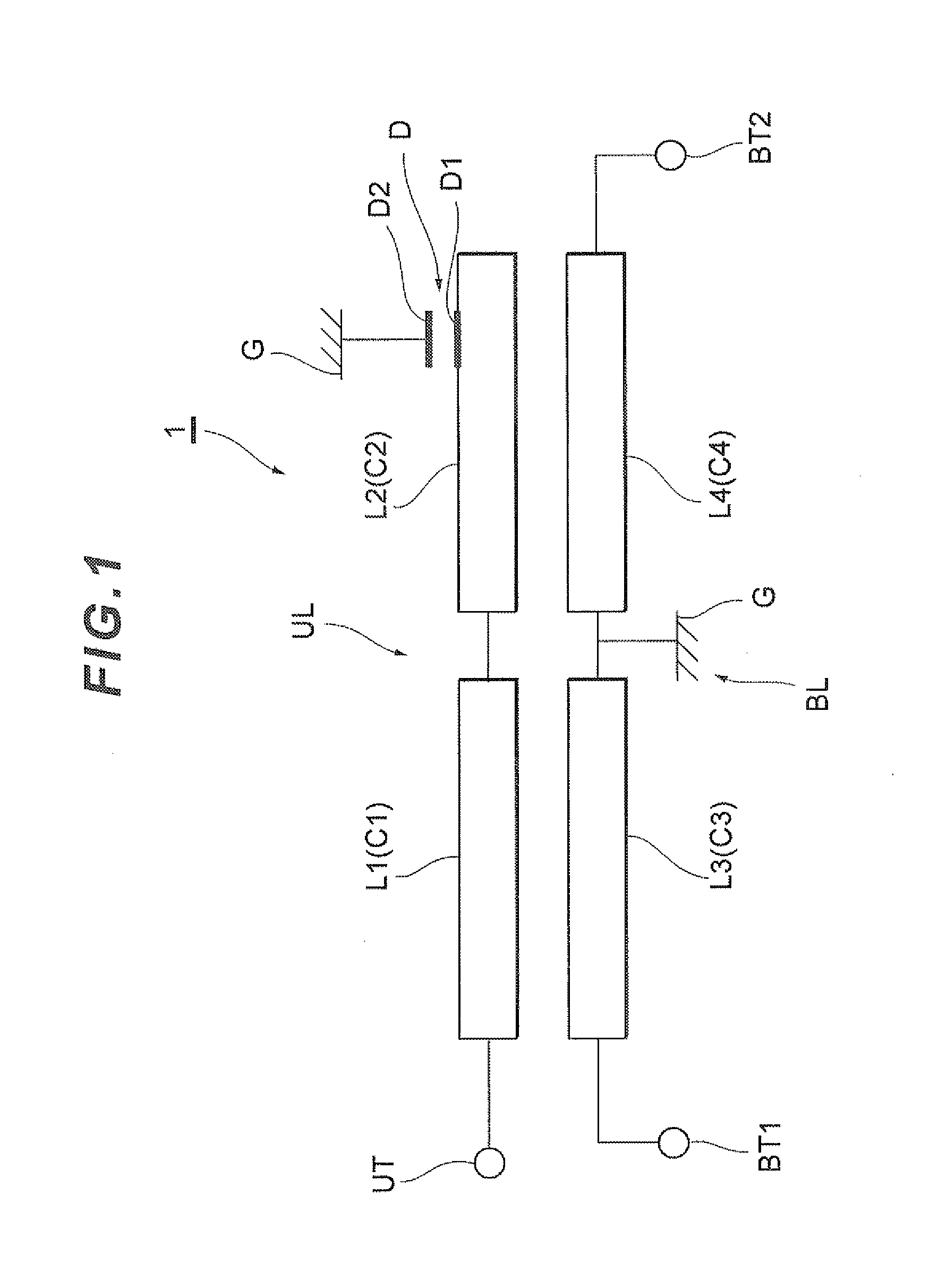
[0164]A thin film balun in a first embodiment corresponding to the first aspect of the present invention is described first. FIG. 1 is an equivalent circuit diagram showing a structure of the thin film balun in the first embodiment of the present invention. A thin film balun 1 includes an unbalanced transmission line (unbalanced circuit) UL in which a line portion L1 (first line portion) and a line portion L2 (second line portion) are connected in series, and a balanced transmission line (balanced circuit) BL in which a line portion L3 (third line portion) and a line portion L4 (fourth line portion) are connected in series. The line portions L1 and L3 form magnetic coupling, and the line portions L2 and L4 form magnetic coupling.
[0165]In the thin film balun 1, an end of the line portion L1 other than an end connected to the line portion L2 is connected to an unbalanced terminal UT, and a part of an end of the line portion L2 other than an end connected to the line portion L1 is conn...
example 2e
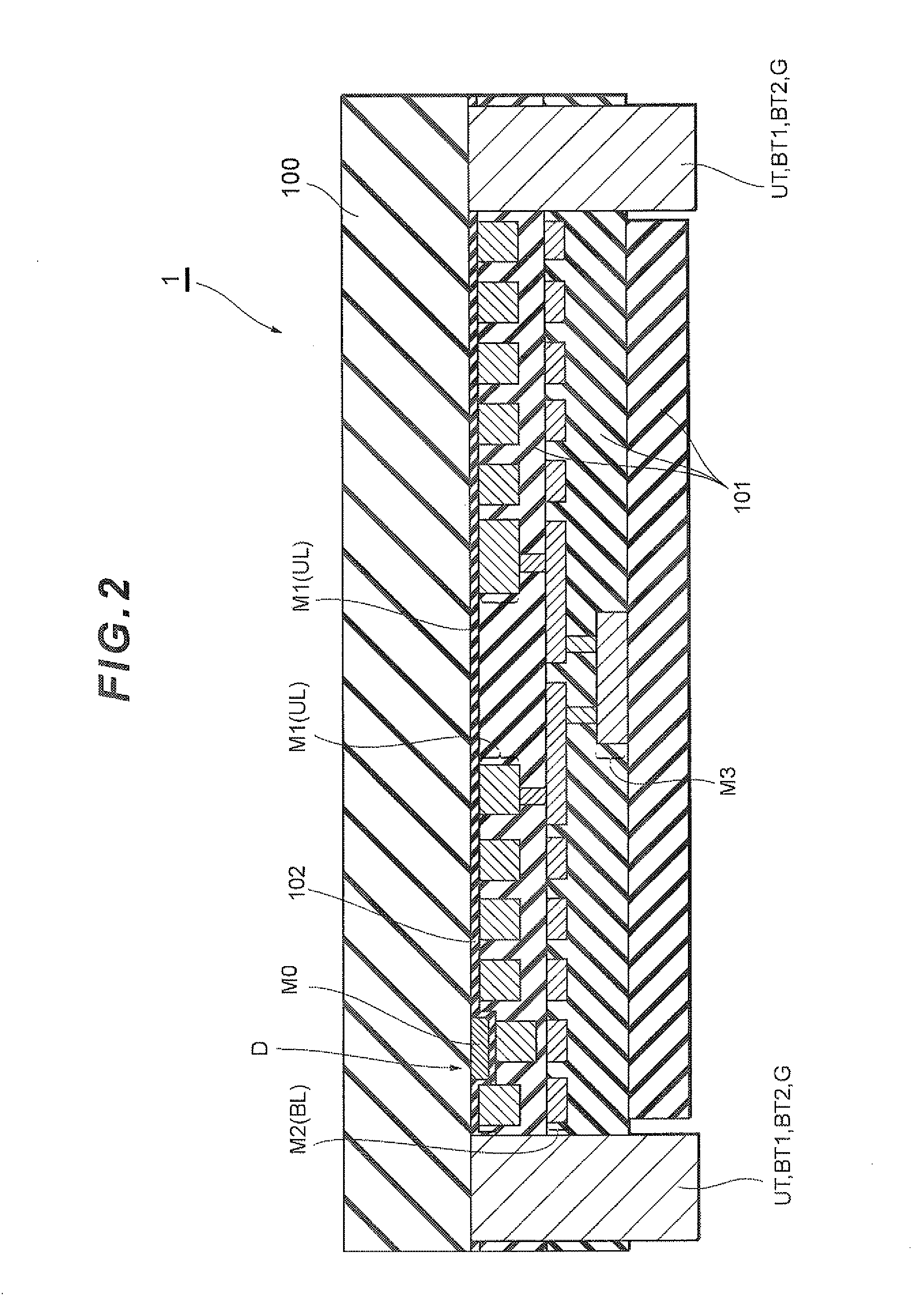
[0188]FIG. 17 is a horizontal sectional view schematically showing the wiring layer M0 of a thin film balun 2B of an example 2B. Structures other than the wiring layer M0 are the same as those in the example 2. In the thin film balun 2B shown in FIG. 17, the electrode D2 of the capacitor D is positioned so as to be parallel to an extending direction of a space between the coil conductors of the second and third lines from the bottom of the coil portion C2 and face a part of the coil conductors on both sides of the space in plan view.
example 2c
[0189]FIG. 18 is a horizontal sectional view schematically showing the wiring layer M0 of a thin film balun 2C of an example 2C. Structures other than the wiring layer M0 are the same as those in the example 2. In the thin film balun 2C shown in FIG. 18, the electrode D2 of the capacitor D is positioned so as to be parallel to an extending direction of a space between the coil conductor of the first line (the extension 12c) and the coil conductor of the second line from the bottom of the coil portion C2 and face a part of the coil conductors on both sides of the space in plan view.
PUM
 Abstract
Description
Claims
Application Information
 - R&D
- Intellectual Property
- Life Sciences
- Materials
- Tech Scout
- Unparalleled Data Quality
- Higher Quality Content
- 60% Fewer Hallucinations
Browse by: Latest US Patents, China's latest patents, Technical Efficacy Thesaurus, Application Domain, Technology Topic, Popular Technical Reports.
© 2025 PatSnap. All rights reserved.Legal|Privacy policy|Modern Slavery Act Transparency Statement|Sitemap|About US| Contact US: help@patsnap.com


