
Method for manufacturing a sensor component and sensor component

a manufacturing method and sensor technology, applied in the direction of fluid pressure measurement, fluid pressure measurement by electric/magnetic elements, instruments, etc., can solve the problems of strain gauge failure, detachment from damage to the bond of the strain gauge with the rest of the sensor component, so as to avoid or at least reduce the disadvantages of the related art, avoid failures or reduce the effect of failures

Inactive Publication Date: 2010-09-02
ROBERT BOSCH GMBH
View PDF4 Cites 18 Cited by
  • Summary
  • Abstract
  • Description
  • Claims
  • Application Information

AI Technical Summary

Benefits of technology

[0002]A method according to the present invention for manufacturing a sensor component and the sensor component according to the present invention are advantageous in that, by using a low-temperature step for producing the bond between a semiconductor substrate and a metal substrate, the disadvantages of the related art are avoided or at least reduced. In particular, no or fewer shrink cavities or inclusions are present in a bonding material and no or fewer thermomechanical stresses are present in a bonding layer. It is possible according to the present invention that occurrences of failures are avoided or reduced and, moreover, that an improved as well as simplified and, thus, more cost-effective manufacturing flow is achieved. According to the present invention, higher stress reversal strength, and, moreover, great strength of the bond—even at comparatively high temperatures of more than 250° C.—may also be achieved.
[0003]According to the present invention, it may be preferable that that prior to a first step, a metal plating layer is applied to the semiconductor substrate and / or to the metal substrate. This makes it possible to improve the bond of the metal substrate with the semiconductor substrate in an advantageous manner. In particular, bonding characteristics of the bonding material with the respective adjacent substrate material may be improved.
[0004]Furthermore, it may be preferable that, prior to a second step, the bonding material is provided as a powdery or paste-like material or that the bonding material has metal particles and, furthermore, additives, in particular ground waxes, and that the additives constitute a comparatively small proportion of the bonding material. This makes it possible that the bonding material may be created to be particularly well processable so that the manufacturing process according to the present invention may be devised to be particularly cost-effective, simple, and comparatively straightforward.
[0007]According to the present invention it may also be preferable that, during the second step, the metal substrate and the semiconductor substrate are pressed together with the aid of a force which substantially exceeds the semiconductor substrate's own weight or, alternatively, are pressed together using a force which is essentially formed only by the metal substrate's or the semiconductor substrate's own weight, thereby producing optimal bonding of the substrates depending on the intended process sequence or depending on the bonding material used.

Problems solved by technology

The method has the disadvantage that, for joining the strain gauges with the rest of the sensor component, low melting glass (seal glass) is applied to at least one surface to be bonded and the joined system is heated.
On the one hand, it is necessary here to provide a comparatively high process temperature of, for example, approximately 440° C. or higher and, on the other hand, there is frequently the problem that inclusions (so called shrink cavities) are embedded in the seal glass layer which have a detrimental effect on the bond of the strain gauge with the rest of the sensor component.
Furthermore, the comparatively high process temperature may cause comparatively high mechanical stresses during manufacture of the bond which may result in the strain gauge failing (for example, due to failure of the analyzing electronics) or becoming detached from the rest of the sensor component.

Method used


Image

  • Method for manufacturing a sensor component and sensor component
  • Method for manufacturing a sensor component and sensor component
  • Method for manufacturing a sensor component and sensor component

Examples


Embodiment Construction

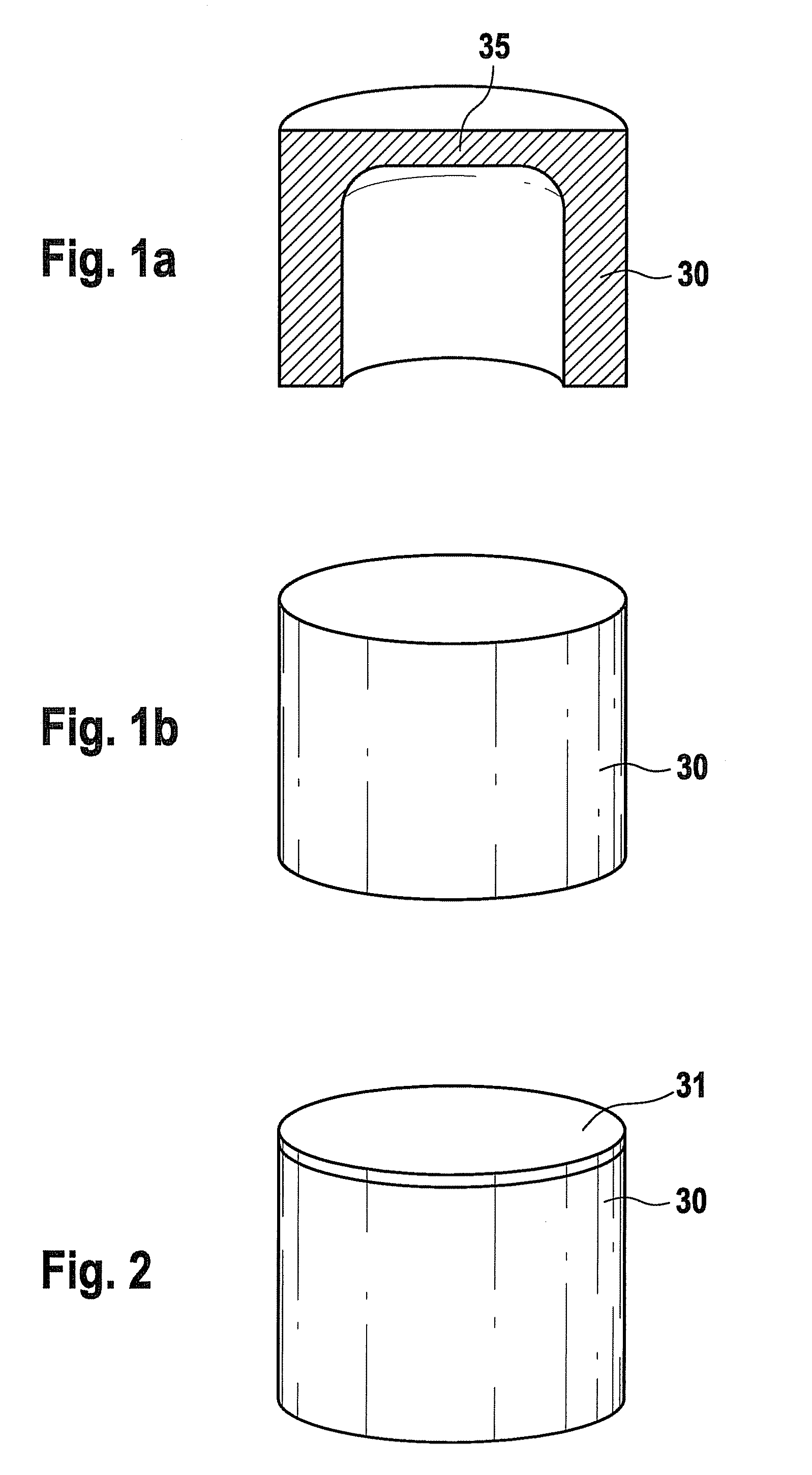
[0013]FIGS. 1a and 1b respectively show a schematic sectional view and a perspective view of a metal substrate 30. Metal substrate 30 has an essentially cylindrical shape. The cylinder, starting from a front face, has a recess along its longitudinal axis and the other front face is closed and forms a sensor diaphragm 35, e.g., for forming a pressure sensor. It may be provided that sensor diaphragms 35 of different thicknesses are used for sensing different pressure ranges. A pressure state present in the interior of the cylinder, i.e., in the recess, exerts a pressure force on the front face of metal substrate 30, thereby curving sensor diaphragm 35. A semiconductor substrate 20 (not shown in FIG. 1), bonded with metal substrate 30 on the sensor diaphragm 35, is able to detect a curvature of sensor diaphragm 35. For this purpose, a bond between semiconductor substrate 20 and metal substrate 30 via a bonding material 40 (not shown in FIG. 1) is produced in a low temperature process w...


PUM

PropertyMeasurementUnit
Lengthaaaaaaaaaa
Nanoscale particle sizeaaaaaaaaaa
Temperatureaaaaaaaaaa

Abstract

A method for manufacturing a sensor component and a sensor component. The sensor component has a semiconductor substrate and a metal substrate. The semiconductor substrate and the metal substrate are bonded together with the aid of a low-temperature process. A bonding material containing metal particles is applied in a first step to the semiconductor substrate and / or the metal substrate and a sintering process is used in a second step for producing the bond between the semiconductor substrate and the metal substrate.

Description

BACKGROUND INFORMATION[0001]A method for manufacturing deformation sensors having a strain gauge and for manufacturing strain gauges and deformation sensors is known from published German patent document DE 101 56 406. The method has the disadvantage that, for joining the strain gauges with the rest of the sensor component, low melting glass (seal glass) is applied to at least one surface to be bonded and the joined system is heated. On the one hand, it is necessary here to provide a comparatively high process temperature of, for example, approximately 440° C. or higher and, on the other hand, there is frequently the problem that inclusions (so called shrink cavities) are embedded in the seal glass layer which have a detrimental effect on the bond of the strain gauge with the rest of the sensor component. Furthermore, the comparatively high process temperature may cause comparatively high mechanical stresses during manufacture of the bond which may result in the strain gauge failing...

Claims


Application Information

Patent Timeline
IPC IPC(8): H01L29/66B32B37/06
CPCG01L9/0042H01L24/28H01L24/31H01L24/83H01L2224/29339H01L2224/83101H01L2924/01006H01L2224/8384H01L2924/0102H01L2924/01078H01L2924/01079H01L24/29H01L2224/83801H05K3/00H05K1/00G01L9/00
Inventor DONIS, DIETER
Owner ROBERT BOSCH GMBH
Learn More