
Bulk thermoelectric material and thermoelectric device comprising the same

a thermoelectric material and thermoelectric device technology, applied in the direction of thermoelectric device junction materials, material nanotechnology, electrical apparatus, etc., can solve the problems of low energy conversion efficiency, limited range of zt, and decrease of other

Inactive Publication Date: 2010-05-06
CHUNGJU NAT UNIV IND ACADEMIC COOPERATION +1
View PDF4 Cites 43 Cited by
  • Summary
  • Abstract
  • Description
  • Claims
  • Application Information

AI Technical Summary

Benefits of technology

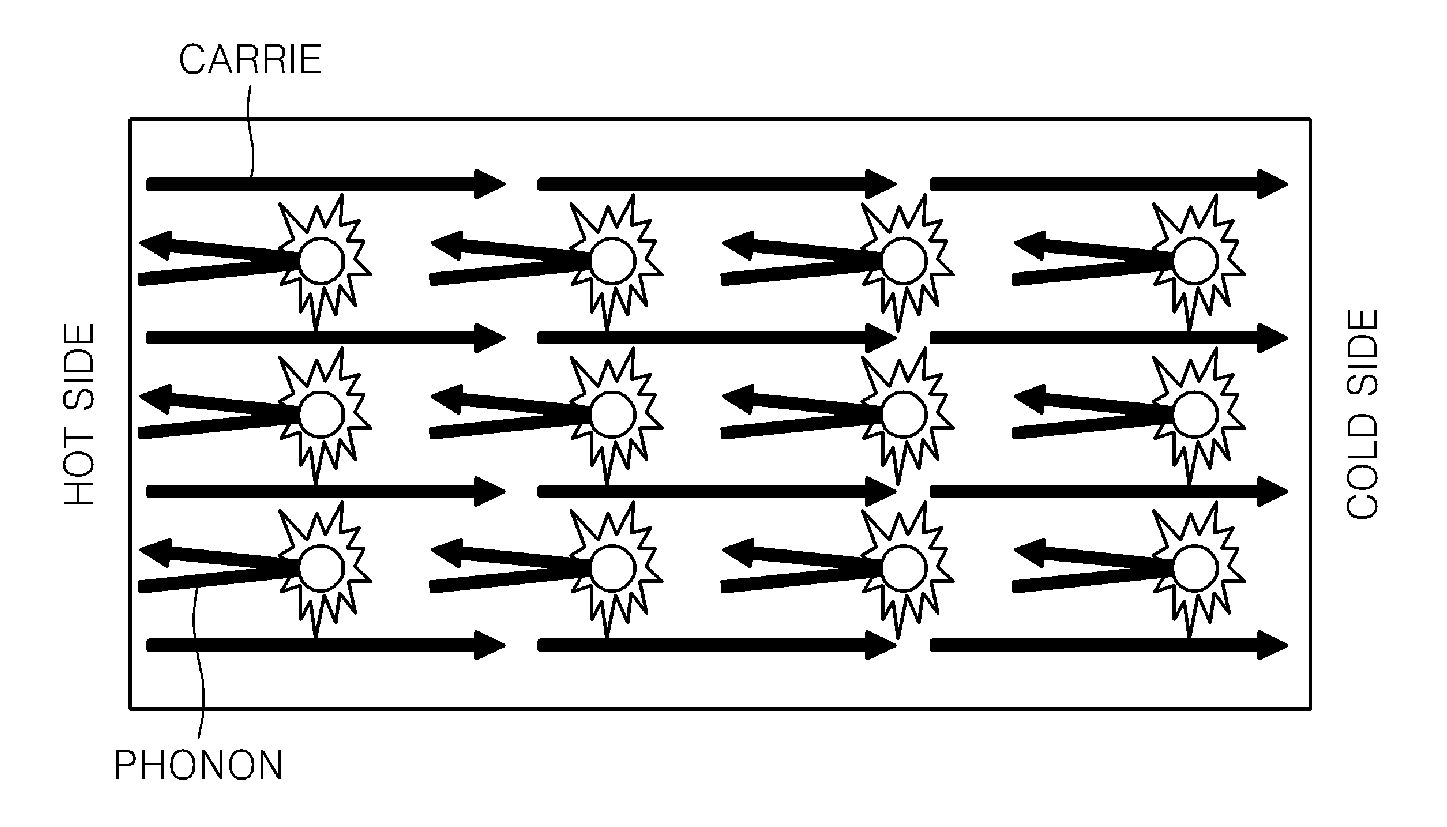
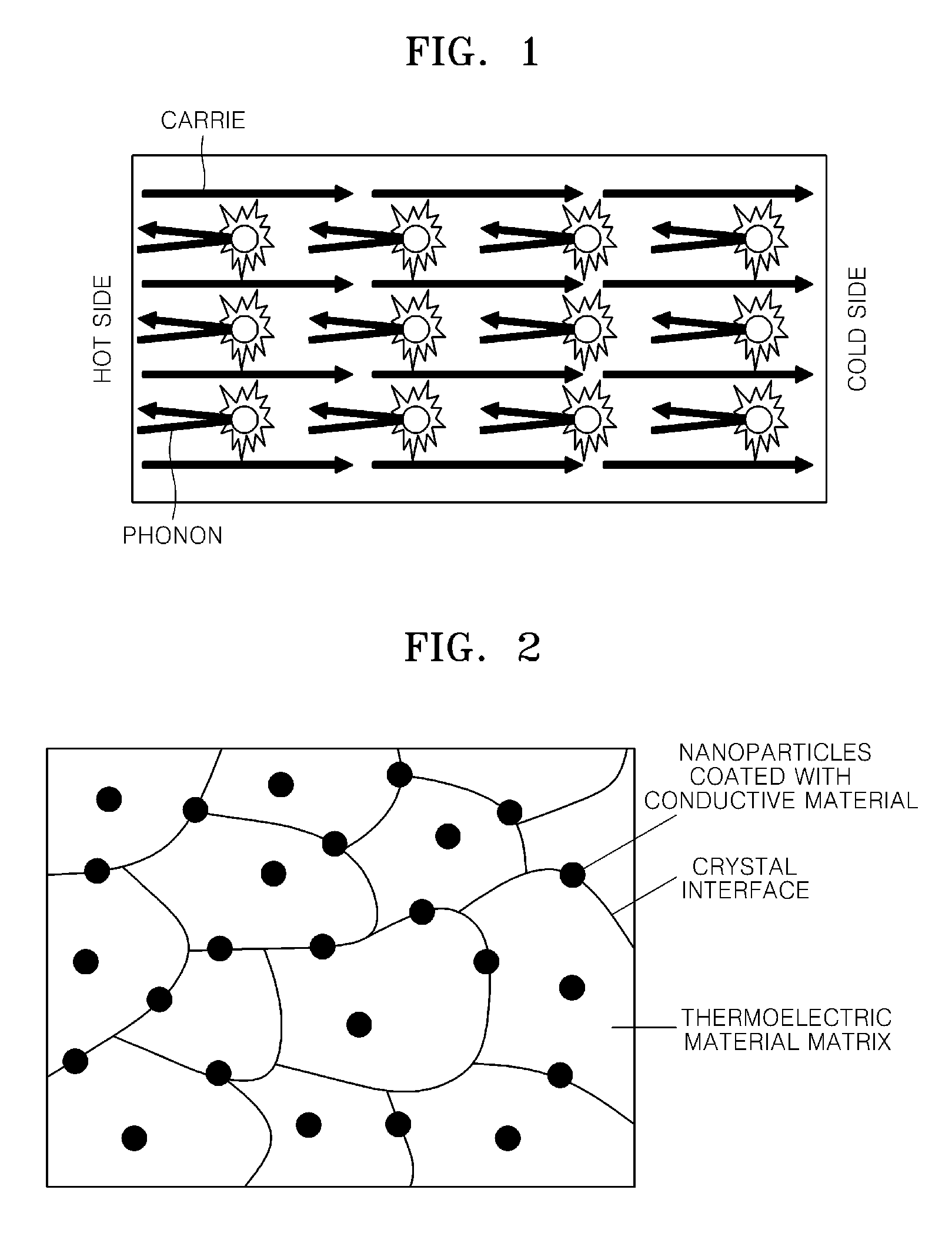
The patent describes a new type of thermoelectric material that has nanoparticles embedded in a crystalline matrix. These nanoparticles are coated with a conductive material, which helps to scatter phonons and allow electrons to move freely. This results in a material that has better performance as a thermoelectric device. The nanoparticles can be metal or ceramic particles, and their size is similar to the size of phonons (the particles that carry heat in the material). The conductive material coating can be about the same size as the phonons, and the volume of the nanoparticles can be between 0.5% and 15% of the total material volume. This new material could be used in thermoelectric devices to improve their performance.

Problems solved by technology

Low energy conversion efficiency is a significant factor inhibiting the application of thermoelectric materials in thermoelectric cooling and power generation.
However, the value of ZT has a limited range since the electrical conductivity and the Seebeck coefficient have a trade-off relationship by which when one of the electrical conductivity or the Seebeck coefficient is increased, the other is decreased.

Method used


Image

  • Bulk thermoelectric material and thermoelectric device comprising the same
  • Bulk thermoelectric material and thermoelectric device comprising the same
  • Bulk thermoelectric material and thermoelectric device comprising the same

Examples


example 1

[0079]1-1: Preparation of C-Coated TiO2 nanoparticles

[0080]Powder of TiO2 nanoparticles having a mean diameter of about 7 nm and phosphoric acid ethoxylated nonylphenyl ether, represented by Formula 1 below, as a phosphate surfactant were added to ethyl acetate solvent, and the solution was ultrasonically stirred for 30 minutes. The solvent was completely volatilized using a rotary vacuum evaporator in a constant-temperature bath at 60° C. to obtain dried powder. Then, the resultant was heat-treated at 350° C. for 1 hour and pulverized to prepare a powder of titanium oxide (C-coated TiO2) nanoparticles, on which a layer of conductive material including carbon and a small amount of phosphate and having a thickness of 3 nm or less was formed, having a mean diameter D50 of about 7 to about 10 nm. FIG. 6 is a transmission electron microscope (“TEM”) image of the prepared nanoparticles coated with the conductive material. FIG. 7 is a graph illustrating the results of the energy dispersiv...

example 2

[0084]Thermoelectric materials were prepared in the same manner as in Example 1, except that 1% by volume and 5% by volume of the powder of nanoparticles were respectively used instead of 3% by volume of the powder of nanoparticles used in operation 1-1 of Example 1.

example 3

[0085]A thermoelectric material was prepared in the same manner as in Example 1, except that a mixture including TiO2, SiO2, Al2O3, and ZrO2 was used instead of the TiO2 nanoparticles used to prepare the nanoparticles in operation 1-1 of Example 1.


PUM

PropertyMeasurementUnit
thicknessaaaaaaaaaa
diameteraaaaaaaaaa
thicknessaaaaaaaaaa

Abstract

A bulk thermoelectric material having a structure in which migration of carriers is not inhibited but phonons are scattered is described. The bulk thermoelectric material includes: a bulk crystalline thermoelectric material matrix; and nanoparticles coated with a conductive material within the thermoelectric material matrix.

Description

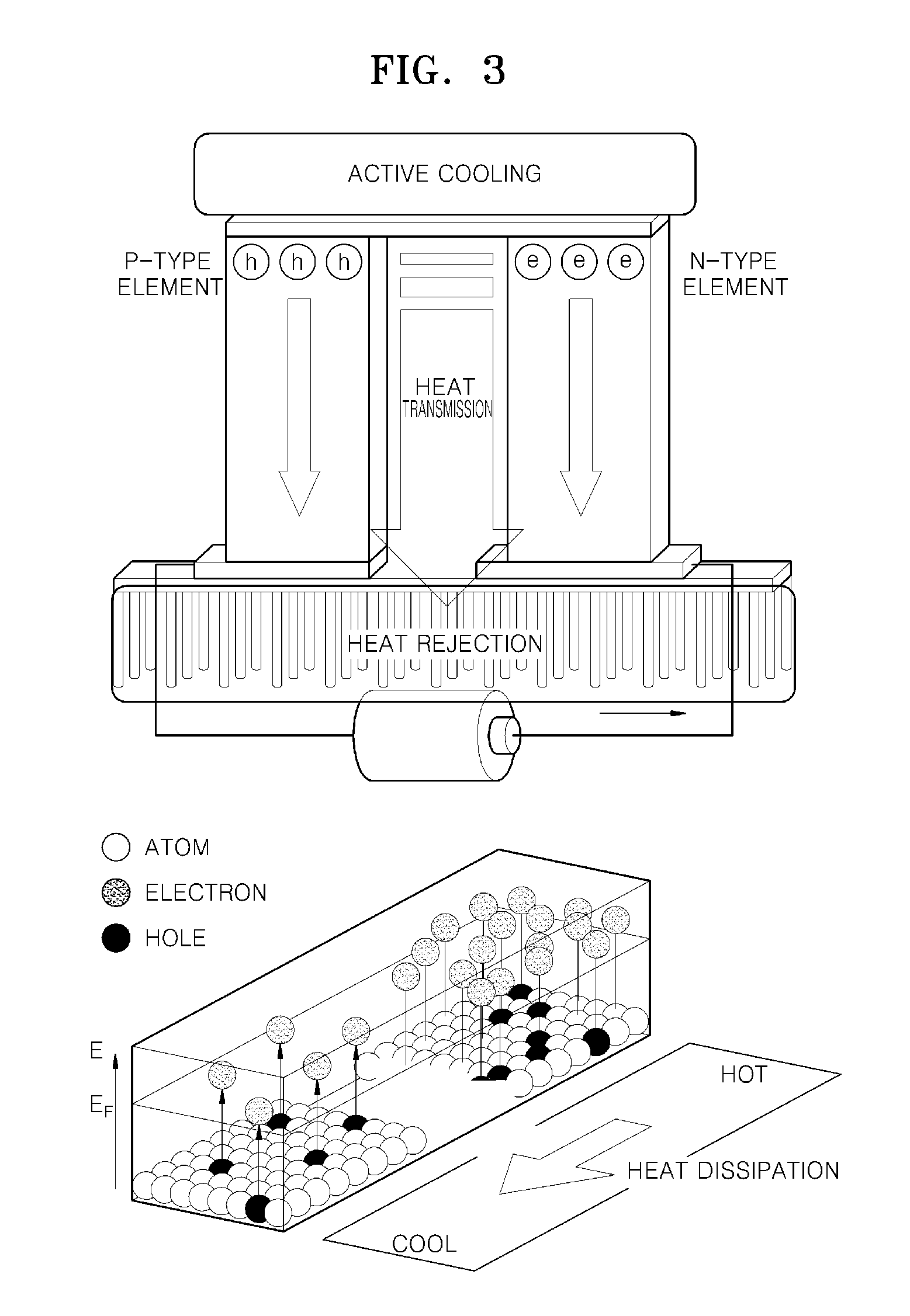
CROSS-REFERENCE TO RELATED APPLICATIONS[0001]This application claims priority to Korean Patent Application No. 10-2008-0104263, filed on Oct. 23, 2008, and all the benefits accruing therefrom under 35 U.S.C. §119, the contents of which in its entirety are herein incorporated by reference.BACKGROUND[0002]1. Field[0003]This disclosure relates to a bulk thermoelectric material having excellent thermoelectric energy conversion efficiency and more particularly, to a thermoelectric material including a bulk crystalline thermoelectric material matrix and nanoparticles.[0004]2. Description of the Related Art[0005]The thermoelectric effect is a reversible and direct conversion of a temperature difference to electric voltage and vice versa, caused by the migration of electrons and holes. The thermoelectric effect encompasses the Peltier effect, which is a temperature difference created by supplying currents to two ends of a thermoelectric material, and which is generally applied to cooling sy...

Claims


Application Information

Patent Timeline
Patent Type & Authority Applications(United States)
IPC IPC(8): H01L35/12H10N10/00H10N10/85
CPCH01L35/16H01L35/26H10N10/857H10N10/852B82Y30/00H10N10/00
Inventor LEE, KYU-HYOUNGLEE, SANG-MOCKLEE, EUN-SUNGKIM, IL-HO
Owner CHUNGJU NAT UNIV IND ACADEMIC COOPERATION
Learn More