Ultrasonic probe and ultrasonic diagnostic apparatus using the same
a technology of ultrasonic probes and diagnostic equipment, applied in diagnostics, mechanical vibration separation, medical science, etc., can solve problems such as deterioration in insulation construction and insufficient insulation, and achieve the effect of preventing electric leakage to an obj
- Summary
- Abstract
- Description
- Claims
- Application Information
AI Technical Summary
Benefits of technology
Problems solved by technology
Method used
Image
Examples
embodiment 1
[0065]Next, embodiment 1 of the present invention will be described referring to FIG. 5 and FIG. 6.
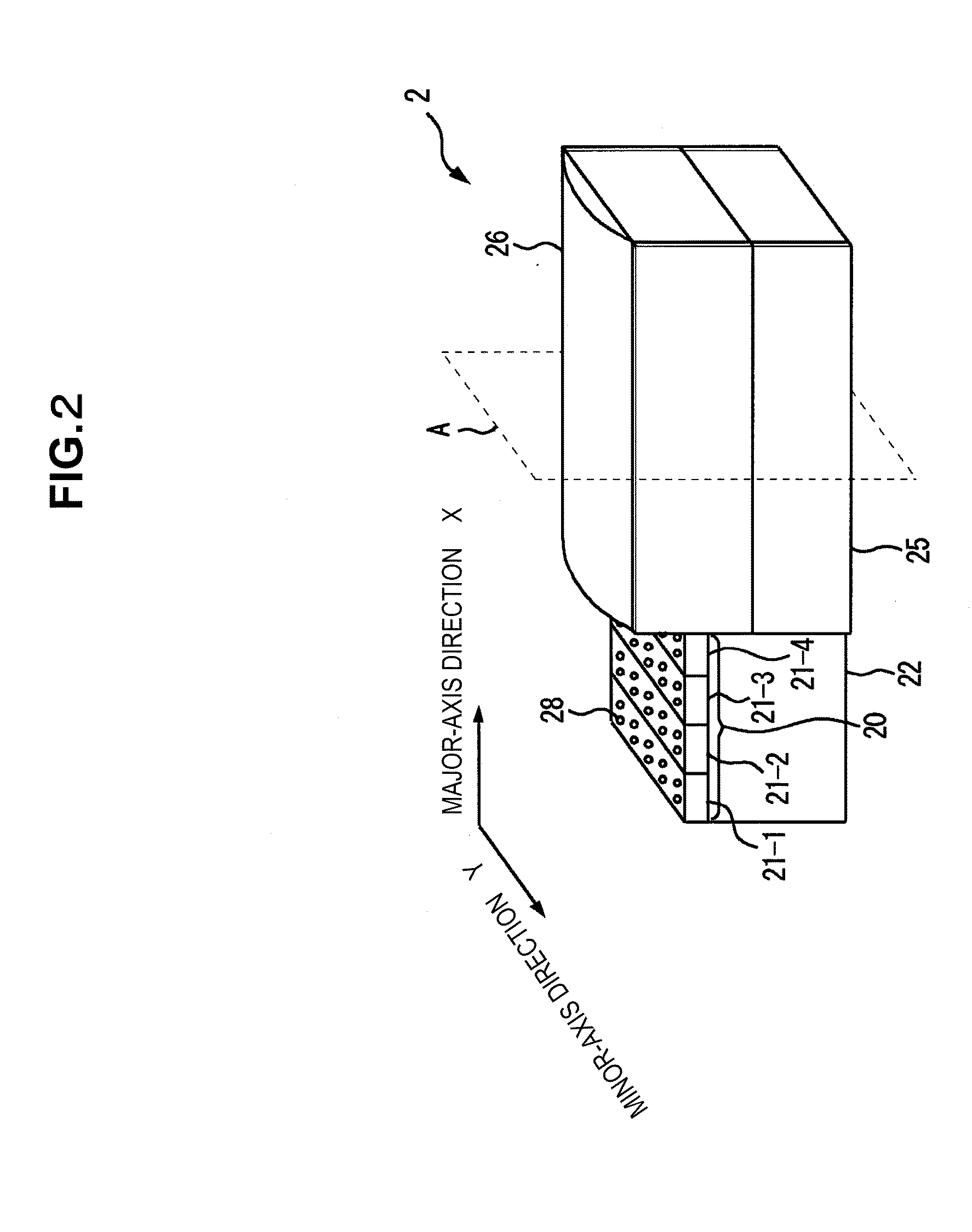
[0066]FIG. 5 shows the ultrasonic probe 2 related to embodiment 1. FIG. 5 is a cross-sectional view of the flat plane “A” of the ultrasonic probe 2 shown in FIG. 2.
[0067]In accordance with FIG. 5, an insulating film 78 which is an insulation layer is formed on the back surface of the acoustic lens 26. The insulating film 78 is, for example, a silicon oxide film or a paraxylene film.
[0068]The cMUT chip 20 is glued to the upper surface of the backing layer22 via the adhesion layer 70. A flexible substrate 72 (Flexible printed circuits: FPC) is provided from the peripheral border of the upper surface of the backing layer 22 over to the side surfaces in four directions. The flexible substrate 72 is glued onto the peripheral border of the upper surface of the backing layer 22 via the adhesion layer 71.
[0069]The adhesion layer 70 and the adhesion layer 71 are an adhesive agent formed by, for...
embodiment 2
[0084]Next, embodiment 2 will be described referring to FIG. 7.
[0085]FIG. 7 shows an ultrasonic probe 2a related to embodiment 2. FIG. 7 is equivalent to the cross-sectional view of the flat plane “A” shown in FIG. 2.
[0086]While the insulation film 78 is illustrated as being disposed in the lower surface of the acoustic lens in embodiment 1, the insulation layer which is electric leakage preventing means for preventing the leakage of electricity from the electrode in the cMUT chip to the object is disposed in the upper surface (object side) of the acoustic lens 26 as an insulation film 78a in embodiment 2.
[0087]In this manner, in the ultrasonic probe 2a of embodiment 2, the insulation layer is formed in the upper surface of the acoustic lens. The spacing between the ultrasonic wave transmitting / receiving surface and the cMUT chip is performed with double insulation by the insulation layer (insulation film) and the acoustic lens. Therefore, even when friction or damage is caused in t...
embodiment 3
[0089]Next, embodiment 3 will be described referring to FIG. 8.
[0090]FIG. 8 shows an ultrasonic probe 2b related to embodiment 3. FIG. 8 is equivalent to the cross-sectional view of the flat plane “A” shown in FIG. 2.
[0091]While the insulation film 78 is described as being disposed on the lower surface of the acoustic lens 26 in embodiment 1, the insulation layer which is electric leakage preventing means for preventing the leakage of electricity from the electrode in the cMUT chip to the object is disposed on the upper surface of the cMUT chip 20 as an insulation film 78b in embodiment 3.
[0092]In this manner, in the ultrasonic probe 2b of embodiment 3, the insulation layer is formed on the upper surface of the cMUT chip. In the spacing between the ultrasonic wave transmitting / receiving surface and the cMUT chip, double insulation is performed by the insulation layer and the acoustic lens. Thus the same effect can be performed as embodiment 1.
PUM
 Abstract
Description
Claims
Application Information
 - R&D
- Intellectual Property
- Life Sciences
- Materials
- Tech Scout
- Unparalleled Data Quality
- Higher Quality Content
- 60% Fewer Hallucinations
Browse by: Latest US Patents, China's latest patents, Technical Efficacy Thesaurus, Application Domain, Technology Topic, Popular Technical Reports.
© 2025 PatSnap. All rights reserved.Legal|Privacy policy|Modern Slavery Act Transparency Statement|Sitemap|About US| Contact US: help@patsnap.com


