Semiconductor Device and Method of Forming Lateral Power MOSFET with Integrated Schottky Diode on Monolithic Substrate

Inactive Publication Date: 2009-12-31
GREAT WALL SEMICON CORP
View PDF3 Cites 15 Cited by
  • Summary
  • Abstract
  • Description
  • Claims
  • Application Information

AI Technical Summary

Benefits of technology

[0022]A need exists to minimize the amount of charge build-up within the body diode and the amount of time necessary to remove the build-up charge in order to increase the efficiency of the MOSFET. Accordingly, in one embodiment, the present invention is a monolithic semiconductor device comprising a first substrate and insulating layer formed over the first substrate. A second substrate is disposed over the insulating layer. A power MOSFET with body diode is for

Problems solved by technology

The extraction and neutralization of the body diode charge results in power loss which lowers the power conversion efficiency of the power MOSFET.
The depth of the stored minority carrier charge and long minority carrier lifetime of the substrate increases both trr and Qrr, which increases power loss and lowers the efficiency of power MOSFET 10.
The extra current flow to MOSFET 37 du

Method used


Image

  • Semiconductor Device and Method of Forming Lateral Power MOSFET with Integrated Schottky Diode on Monolithic Substrate
  • Semiconductor Device and Method of Forming Lateral Power MOSFET with Integrated Schottky Diode on Monolithic Substrate
  • Semiconductor Device and Method of Forming Lateral Power MOSFET with Integrated Schottky Diode on Monolithic Substrate

Examples


Example

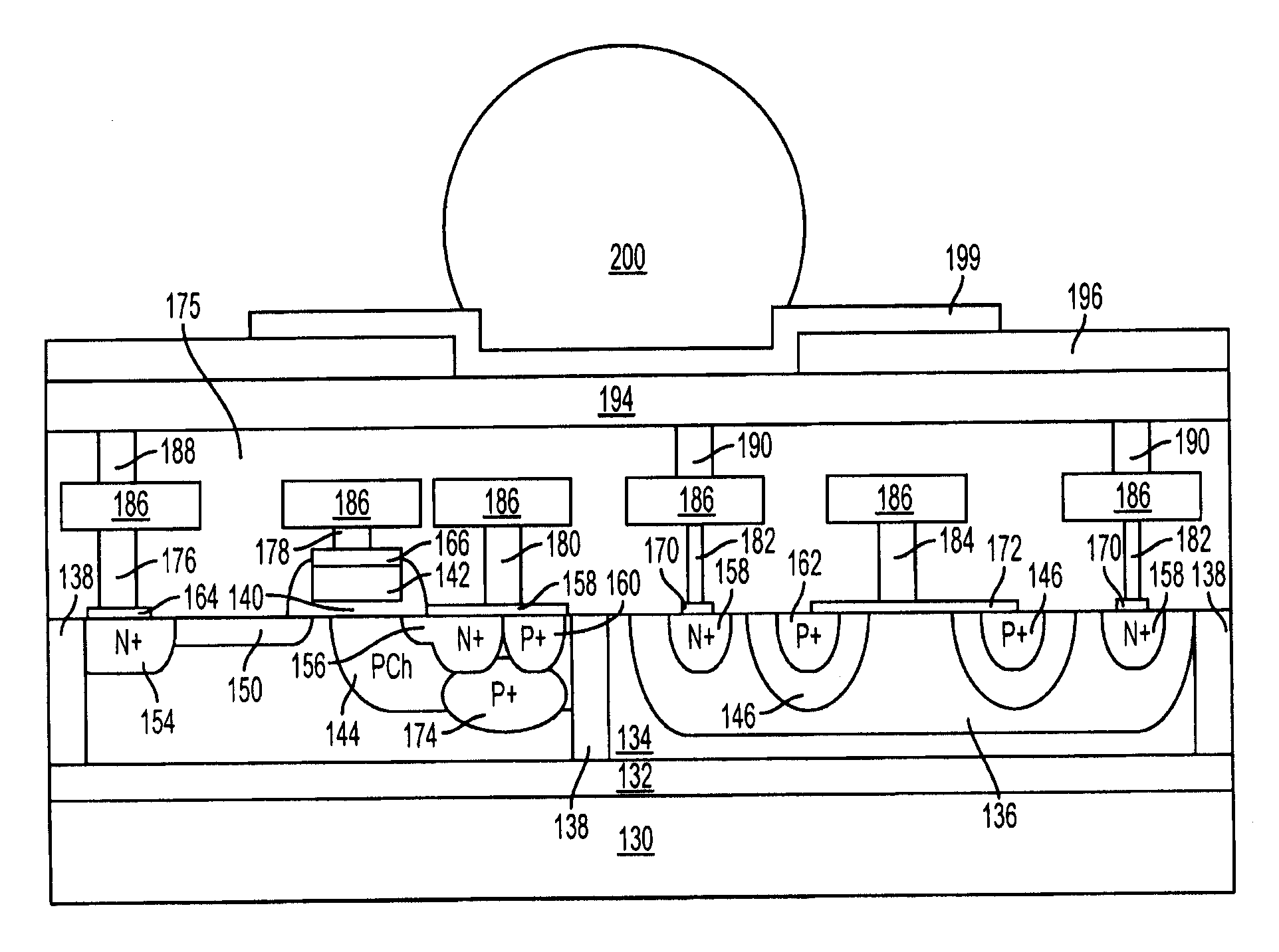
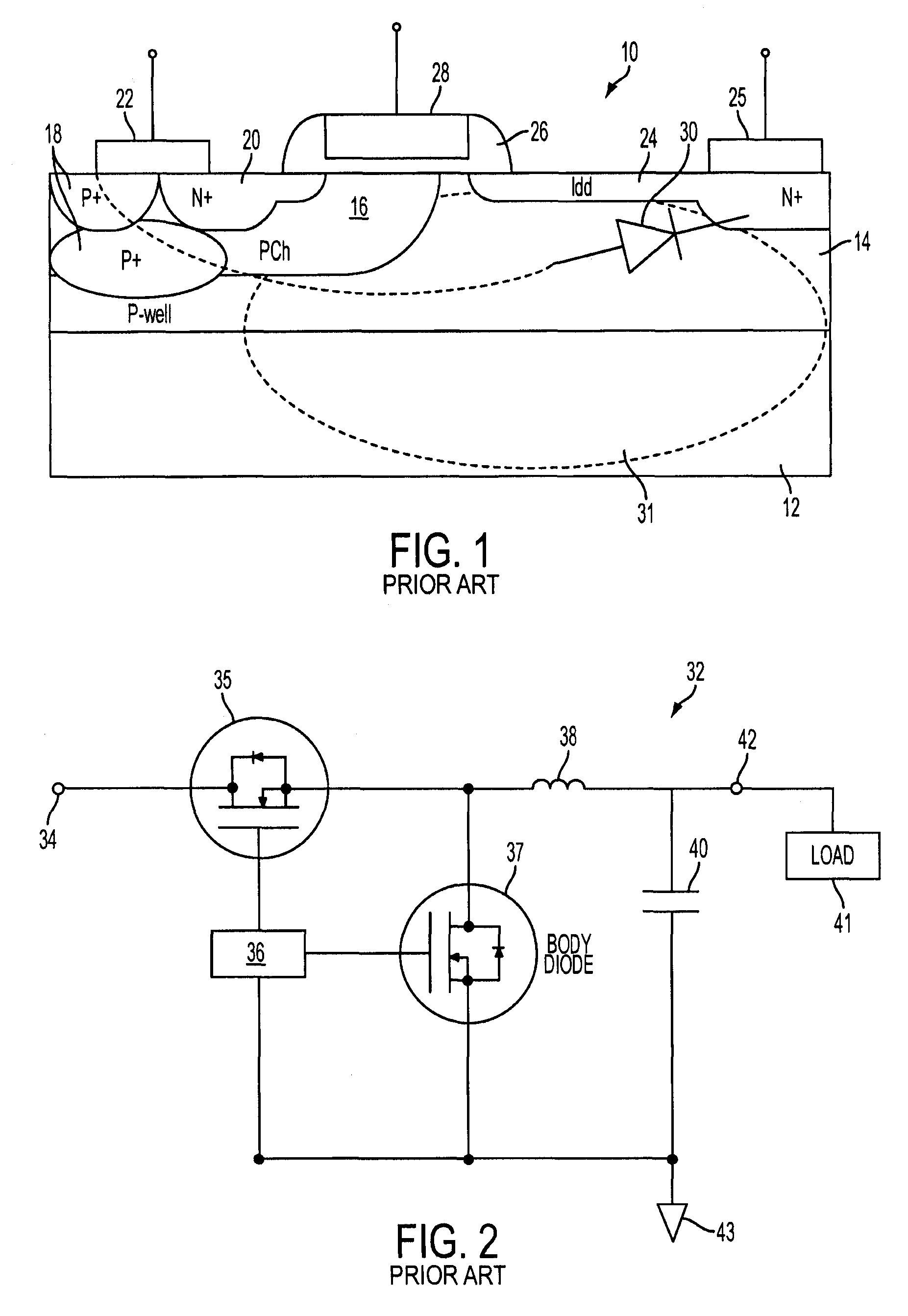
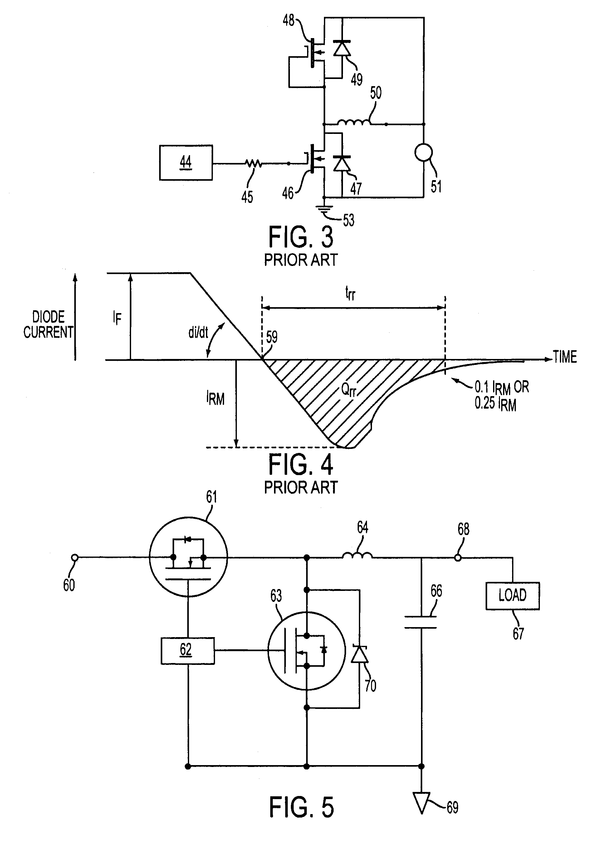
DETAILED DESCRIPTION OF THE DRAWINGS

[0043]The present invention is described in one or more embodiments in the following description with reference to the Figures, in which like numerals represent the same or similar elements. While the invention is described in terms of the best mode for achieving the invention's objectives, it will be appreciated by those skilled in the art that it is intended to cover alternatives, modifications, and equivalents as may be included within the spirit and scope of the invention as defined by the appended claims and their equivalents as supported by the following disclosure and drawings.

[0044]Semiconductor devices are generally manufactured using two complex manufacturing processes: front-end manufacturing and back-end manufacturing. Front-end manufacturing involves the formation of a plurality of die on the surface of a semiconductor wafer. Each die on the wafer contains active and passive electrical components, which are electrically connected to ...


PUM


Abstract

A monolithic semiconductor device has an insulating layer formed over a first substrate. A second substrate is disposed over the first insulating layer. A power MOSFET with body diode is formed over the second substrate. A Schottky diode is formed over the second substrate in proximity to the MOSFET. An insulation trench is formed within the second substrate between the MOSFET and Schottky diode. The isolation trench surrounds the MOSFET and first Schottky diode. A first electrical connection is formed between a source of the MOSFET and an anode of the Schottky diode. A second electrical connection is formed between a drain of the MOSFET and a cathode of the Schottky diode. The Schottky diode reduces charge build-up within the body diode and reverse recovery time of the first power MOSFET. The power MOSFET and integrated Schottky can be used in power conversion or audio amplifier circuit.

Description

CLAIM TO DOMESTIC PRIORITY [0001]The present non-provisional patent application claims priority to provisional application Ser. No. 61 / 075,662, entitled “Lateral Power MOSFET with Integrated Schottky Diode,” filed on Jun. 25, 2008.FIELD OF THE INVENTION [0002]The present invention relates in general to electronic circuits and semiconductor devices and, more particularly, to a semiconductor device and method of forming a lateral power MOSFET with integrated Schottky diode on a monolithic substrate.BACKGROUND OF THE INVENTION [0003]Semiconductor devices are commonly found in modern electronic products. Semiconductor devices vary in the number and density of electrical components. Discrete semiconductor devices generally contain one type of electrical component, e.g., light emitting diode (LED), small signal transistor, resistor, capacitor, inductor, and power metal oxide semiconductor field effect transistor (MOSFET). Integrated semiconductor devices typically contain hundreds to mill...

Claims


Application Information

Patent Timeline
IPC IPC(8): H01L25/07H01L21/328
CPCH01L27/0629H01L27/0727H01L2924/12032H01L2924/12041H01L2924/1306H01L2924/13091H01L2224/04042H01L2924/30107H01L24/13H01L24/05H01L2224/48463H01L29/872H01L29/8611H01L29/47H01L29/66128H01L29/66143H01L2924/00H01L2224/02166H01L2224/11H01L2924/01322H01L2924/12036
Inventor ANDERSON, SAMUEL J.OKADA, DAVID N.SHUMATE, DAVID A.DASHNEY, GARY
Owner GREAT WALL SEMICON CORP
Why Eureka
Try Eureka