MOS Field Effect Transistor and Manufacture Method Therefor
a field effect transistor and metal oxide semiconductor technology, applied in the direction of transistors, semiconductor devices, electrical appliances, etc., can solve the problems of increasing the amount of stress of the si channel layer, increasing the leak current, and increasing the power consumption of the device, so as to increase the ge composition of the buffer sige layer, improve the mobility of electrons and holes, and increase the tensile stress
- Summary
- Abstract
- Description
- Claims
- Application Information
AI Technical Summary
Benefits of technology
Problems solved by technology
Method used
Image

Examples
embodiments
[0046]The present invention is further explained below with reference to embodiments, but the present invention is not limited to the embodiments.
first embodiment
[0047]FIGS. 7A to 7C and FIGS. 8D to 8F are diagrams showing a manufacture process for an MOS field effect transistor according to a first embodiment. FIG. 7A shows a state in which a gate insulating film and a gate electrode are formed in the Si / SiGe lamination, FIG. 7B shows a state in which source / drain regions are etched, and FIG. 7C shows a state in which Si is redoped by CVD. FIG. 8D shows a state in which a sidewall is formed after injection of an extension and an impurity is doped into the source / drain regions, FIG. 8E shows a state in which contact etching stop film is formed, and FIG. 8F shows a state in which an interlayer insulating film is formed, a contact hole is formed therein, and an electrode is formed.
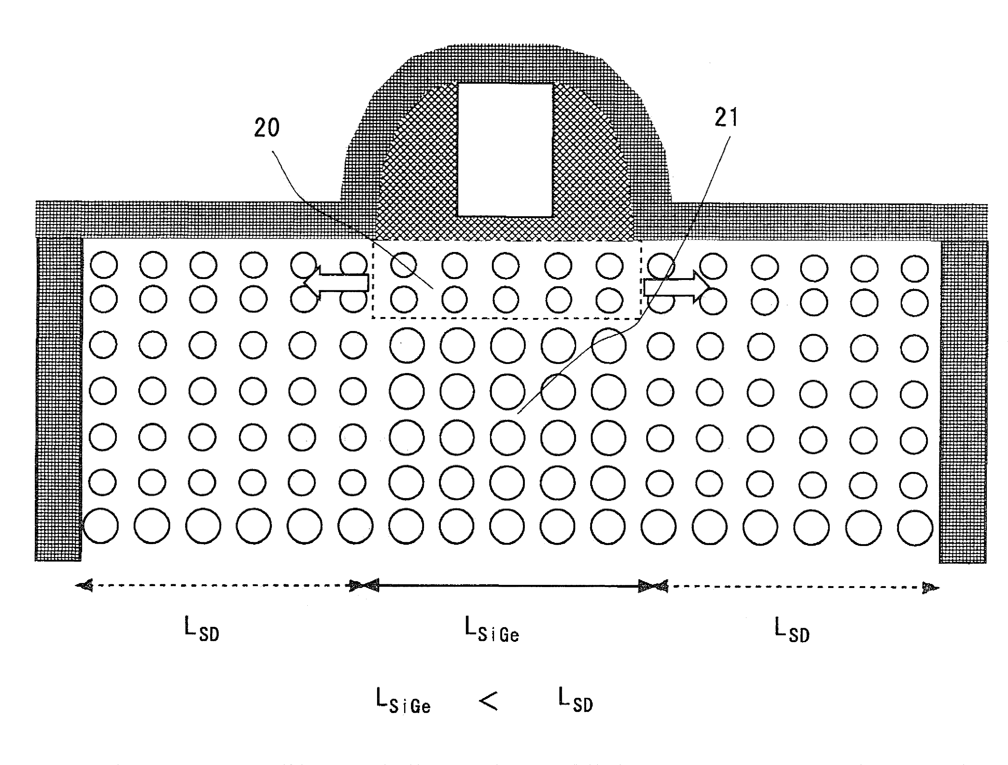
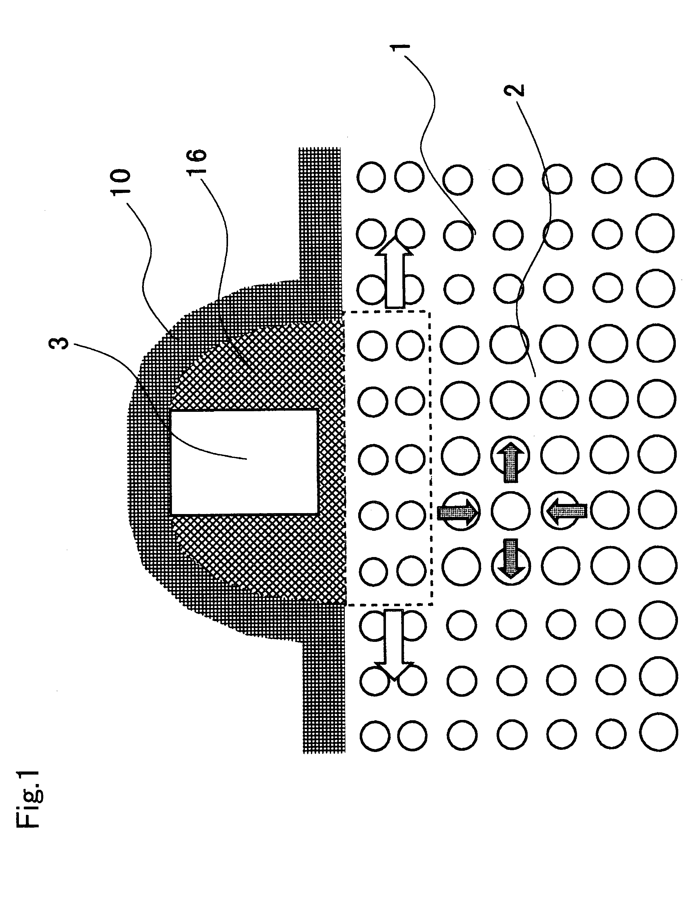
[0048]As shown in FIGS. 7A to 7C, after a device isolation step, a gate insulating film 7 of SiON and the gate electrode 3 of polysilicon are formed on a stressed silicon substrate having the buffer SiGe layer 2. Next, with the gate electrode 3 as a mask, the source / ...
second embodiment
[0051]FIGS. 9A to 9C and FIGS. 10D to 10F are diagrams showing a manufacture process for an MOS field effect transistor according to a second embodiment. FIG. 9A shows a state in which gate insulating film and a gate electrode are formed in the Si / SiGe lamination, FIG. 9B shows a state in which source / drain regions are etched using a gate and a sidewall as a mask, and FIG. 9C shows a state in which Si is redoped by CVD. FIG. 10D shows a state in which a sidewall is formed after injection of an extension, FIG. 10E shows a state in which contact etching stop film is formed on a silicide, and FIG. 10F shows a state in which an interlayer insulating film is formed, a contact hole is formed therein, and an electrode is formed.
[0052]As shown in FIGS. 9A to 9C, after a device isolation step, the gate insulating film 7 of SiON and the gate electrode 3 of polysilicon are formed on a stressed silicon substrate having the buffer SiGe layer 2. Next, the sidewall 16 is formed on the gate electro...
PUM
 Abstract
Description
Claims
Application Information
 - R&D
- Intellectual Property
- Life Sciences
- Materials
- Tech Scout
- Unparalleled Data Quality
- Higher Quality Content
- 60% Fewer Hallucinations
Browse by: Latest US Patents, China's latest patents, Technical Efficacy Thesaurus, Application Domain, Technology Topic, Popular Technical Reports.
© 2025 PatSnap. All rights reserved.Legal|Privacy policy|Modern Slavery Act Transparency Statement|Sitemap|About US| Contact US: help@patsnap.com