Electromagnectic wave detecting element
a technology of electromagnetic waves and elements, applied in the direction of electrical equipment, semiconductor devices, radio frequency control devices, etc., to prevent the reduction of the efficiency of utilizing electromagnetic waves at the sensor portion
- Summary
- Abstract
- Description
- Claims
- Application Information
AI Technical Summary
Benefits of technology
Problems solved by technology
Method used
Image
Examples
first exemplary embodiment
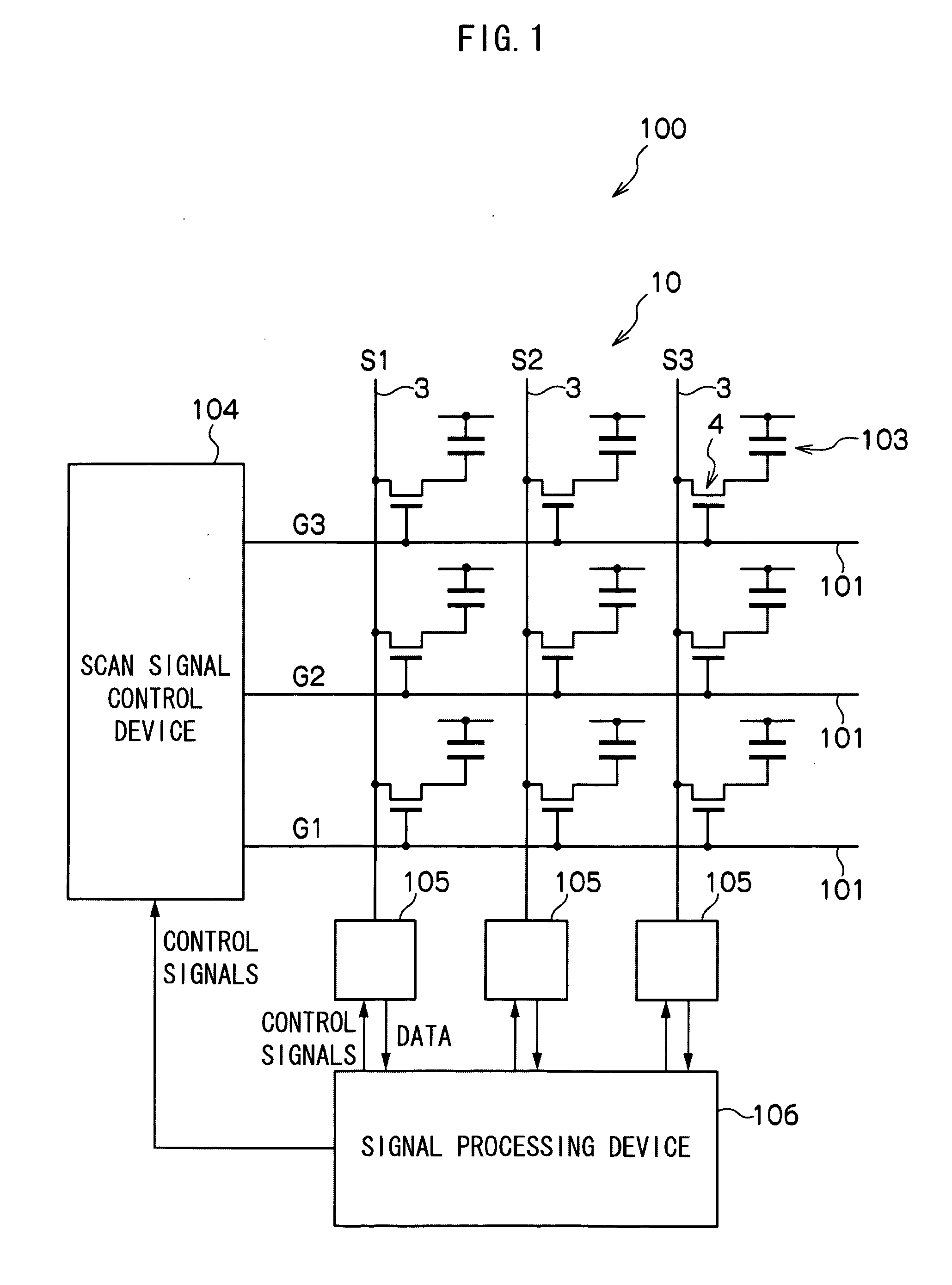
[0058]The overall structure of the radiation image detection device 100 relating to a first exemplary embodiment is illustrated in FIG. 1. However, a scintillator that converts radiation into light is not illustrated.
[0059]As shown in FIG. 1, the radiation image detection device 100 relating to the present exemplary embodiment has an electromagnetic wave detecting element 10.
[0060]The electromagnetic wave detecting element 10 has upper electrode, semiconductor layer, and lower electrode that will be described later. A large number of pixels that are structured to include sensor portions 103 and TFT switches 4 are provided in a two-dimensional form at the electromagnetic wave detecting element 10. The sensor portion 103 receives light, that is obtained by irradiated radiation being converted at a scintillator, and accumulates charges. The TFT switch 4 reads-out the charges accumulated in the sensor portion 103.
[0061]Plural scan lines 101 for turning the TFT switches 4 on and off, and...
second exemplary embodiment
[0098]In a case in which different types of lines are formed at the same wiring layer in the electromagnetic wave detecting element 10, it is easy for leaks to arise between the lines due to poor patterning.
[0099]Thus, a second exemplary embodiment describes a case in which the scan lines 101, the signal lines 3, and the common electrode lines 25 are formed by different wiring layers.
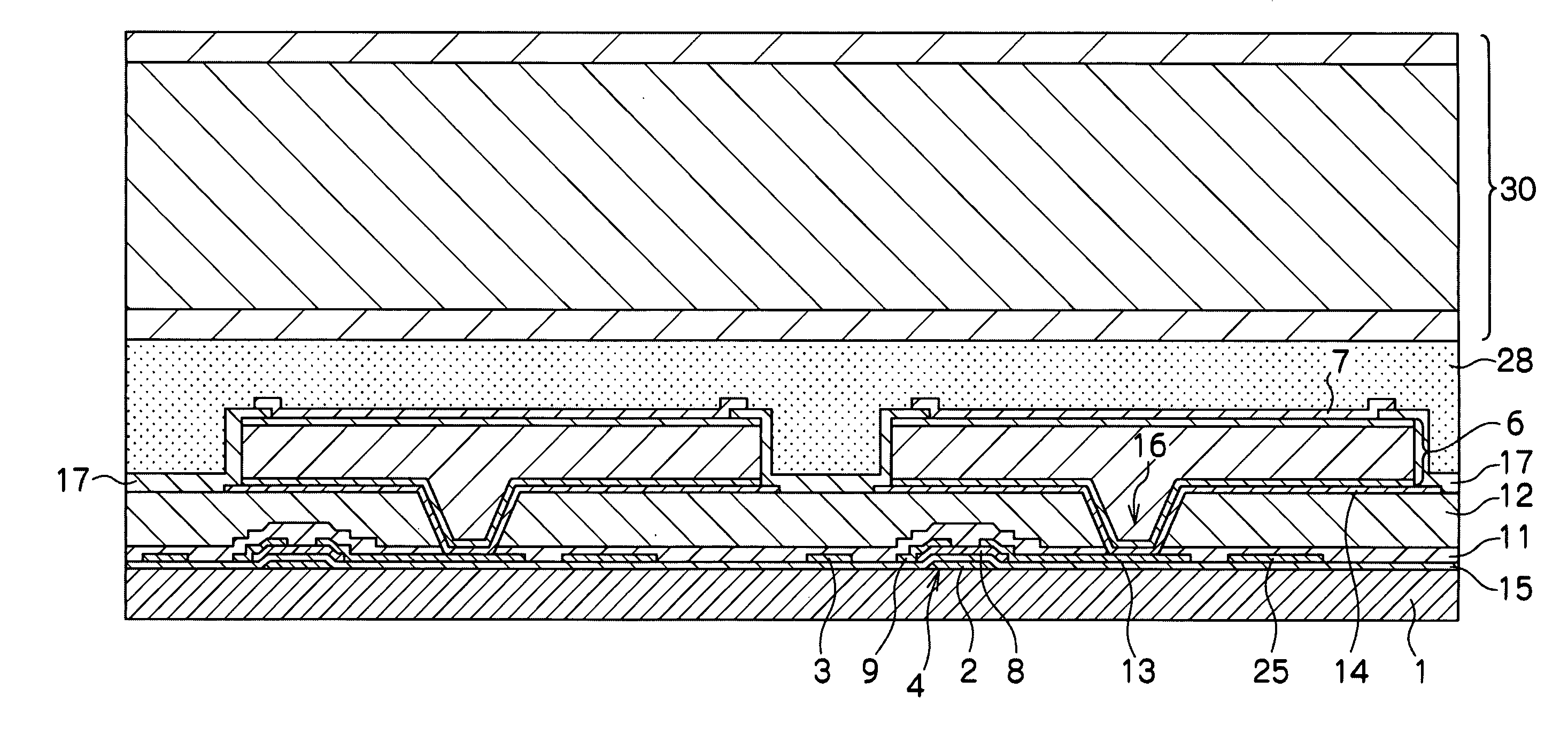
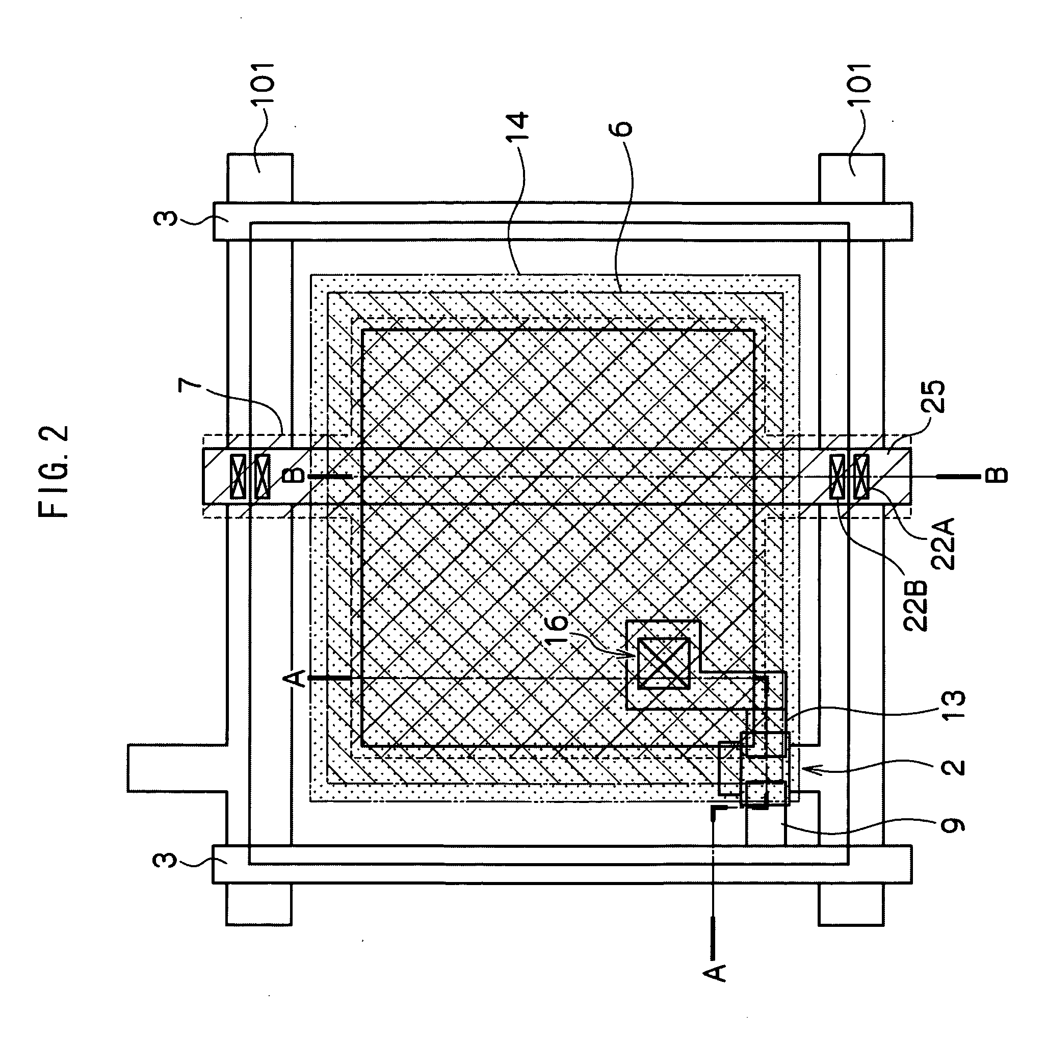
[0100]A plan view showing the structure of one pixel unit of the electromagnetic wave detecting element 10 relating to the second exemplary embodiment is shown in FIG. 6. Further, a cross-sectional view along line A-A of FIG. 6 is shown in FIG. 7A, and a cross-sectional view along line B-B of FIG. 6 is shown in FIG. 7B. Description of portions in FIG. 6 and FIG. 7, that are the same as in FIG. 2 and FIG. 3, is omitted.
[0101]As shown in FIG. 7A and FIG. 7B, at the electromagnetic wave detecting element 10, the scan line 101 and the gate electrode 2 are formed on the substrate 1, and the scan line 101 and...
third exemplary embodiment
[0122]In the first and second exemplary embodiments, the connection regions of the upper electrodes 7 and the common electrode lines 25 are formed on the protective insulating film 17. However, there are cases in which disconnection or the like of the connection regions arises due to changes in the steep angle of the protective insulating film 17 at the lower layer, or cracking, or the like.
[0123]Thus, the third exemplary embodiment describes a case in which an interlayer insulating film 18 is further formed at the peripheries of the respective semiconductor layer 6.
[0124]A plan view showing the structure of one pixel unit of the electromagnetic wave detecting element 10 relating to the third exemplary embodiment is shown in FIG. 17. Further, a cross-sectional view along line A-A of FIG. 17 is shown in FIG. 18A, and a cross-sectional view along line B-B of FIG. 17 is shown in FIG. 18B. Descriptions of portions in FIG. 17 and FIG. 18, that are the same as in FIG. 2 and FIG. 3, are om...
PUM
 Abstract
Description
Claims
Application Information
 - R&D
- Intellectual Property
- Life Sciences
- Materials
- Tech Scout
- Unparalleled Data Quality
- Higher Quality Content
- 60% Fewer Hallucinations
Browse by: Latest US Patents, China's latest patents, Technical Efficacy Thesaurus, Application Domain, Technology Topic, Popular Technical Reports.
© 2025 PatSnap. All rights reserved.Legal|Privacy policy|Modern Slavery Act Transparency Statement|Sitemap|About US| Contact US: help@patsnap.com


